A light-emitting diode epitaxial wafer and its manufacturing method
A technology of light-emitting diodes and manufacturing methods, which is applied to semiconductor devices, electrical components, circuits, etc., can solve problems such as reducing the quality of quantum barrier layer crystals, affecting the crystallization integrity of quantum barrier materials, and reducing the quality of quantum well layer crystals, etc., to achieve reduction Adverse effects, mitigation of adverse effects, effects that favor electromigration
- Summary
- Abstract
- Description
- Claims
- Application Information
AI Technical Summary
Problems solved by technology
Method used
Image
Examples
Embodiment 1
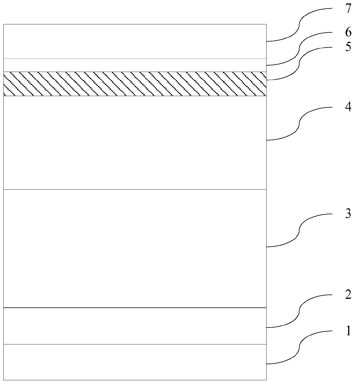
[0033] An embodiment of the present invention provides a light emitting diode epitaxial wafer, see figure 1 , the light-emitting diode epitaxial wafer includes a substrate 1 and a buffer layer 2, an undoped gallium nitride layer 3, an N-type gallium nitride layer 4, a multi-quantum well layer 5, and an electron blocking layer 6 sequentially stacked on the substrate 1 and P-type GaN layer 7 .
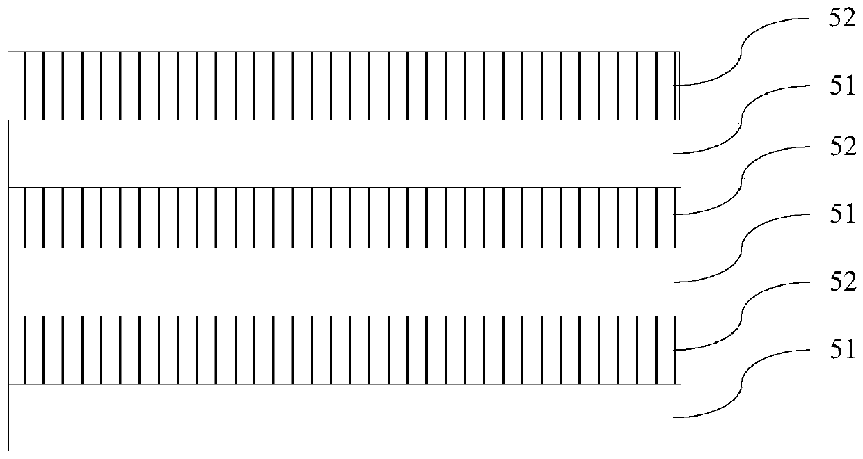
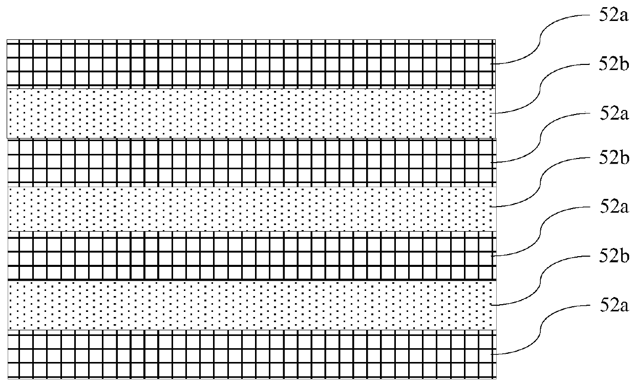
[0034] In this example, see figure 2 , the multi-quantum well layer 5 includes multiple quantum well layers 51 and multiple quantum barrier layers 52, and multiple quantum well layers 51 and multiple quantum barrier layers 52 are stacked alternately. see image 3 , the quantum barrier layer 52 includes (n+1) first sublayers 52a and n second sublayers 52b, n is a positive integer, (n+1) first sublayers 52a and n second sublayers 52b Alternately stacked, the first sub-layer 52a is an undoped gallium nitride layer, and the second sub-layer 52b is a silicon-doped gallium nitride layer. ...
Embodiment 2
[0046] An embodiment of the present invention provides a method for manufacturing a light-emitting diode epitaxial wafer, which is suitable for manufacturing the light-emitting diode epitaxial wafer provided in Embodiment 1, see Figure 4 , the manufacturing method includes:
[0047] Step 201: Provide a substrate.
[0048] Step 202: sequentially growing a buffer layer, an undoped GaN layer, an N-type GaN layer, a multi-quantum well layer, an electron blocking layer and a P-type GaN layer on the substrate.
[0049] In this embodiment, the multi-quantum well layer includes a plurality of quantum well layers and a plurality of quantum barrier layers, the plurality of quantum well layers and the plurality of quantum barrier layers are alternately stacked, and the quantum barrier layer includes (n+1) first sub-layers layer and n second sublayers, n is a positive integer, (n+1) first sublayers and n second sublayers are alternately stacked, the first sublayer is an undoped gallium ...
Embodiment 3
[0061] An embodiment of the present invention provides a method for manufacturing a light-emitting diode epitaxial wafer, and the manufacturing method provided in this embodiment is a specific realization of the manufacturing method provided in Embodiment 2. In this embodiment, Veeco K465i or C4 Metal Organic Chemical Vapor Deposition (English: Metal Organic Chemical Vapor Deposition, abbreviated: MOCVD) equipment is used to realize the manufacture of LED epitaxial wafers. Using high-purity hydrogen (H 2 ) or high-purity nitrogen (N 2 ) or high purity H 2 and high purity N 2 The mixed gas as the carrier gas, high-purity NH 3 As nitrogen source, trimethylgallium (TMGa) and triethylgallium (TEGa) as gallium source, trimethylindium (TMIn) as indium source, trimethylaluminum (TMAl) as aluminum source, silane (SiH4) as N-type dopant, magnesium dicene (CP 2 Mg) as a P-type dopant. The pressure of the reaction chamber is controlled at 100-600 torr.
[0062] Specifically, see ...
PUM
 Abstract
Description
Claims
Application Information


