Chip top protection layer integrity detection device

A technology of integrity detection and protection layer, which is applied in the direction of measuring devices, measuring electricity, and measuring electrical variables, etc., can solve problems such as threats to the information security of integrated circuits, achieve high detection accuracy, and achieve the effect of integrity detection

Active Publication Date: 2019-12-17
TIANJIN UNIV
View PDF4 Cites 0 Cited by
  • Summary
  • Abstract
  • Description
  • Claims
  • Application Information

AI Technical Summary

Problems solved by technology

Therefore, FIB attacks seriously threaten the information security of integrated circuits

Method used


Image

  • Chip top protection layer integrity detection device
  • Chip top protection layer integrity detection device
  • Chip top protection layer integrity detection device

Examples


Embodiment Construction

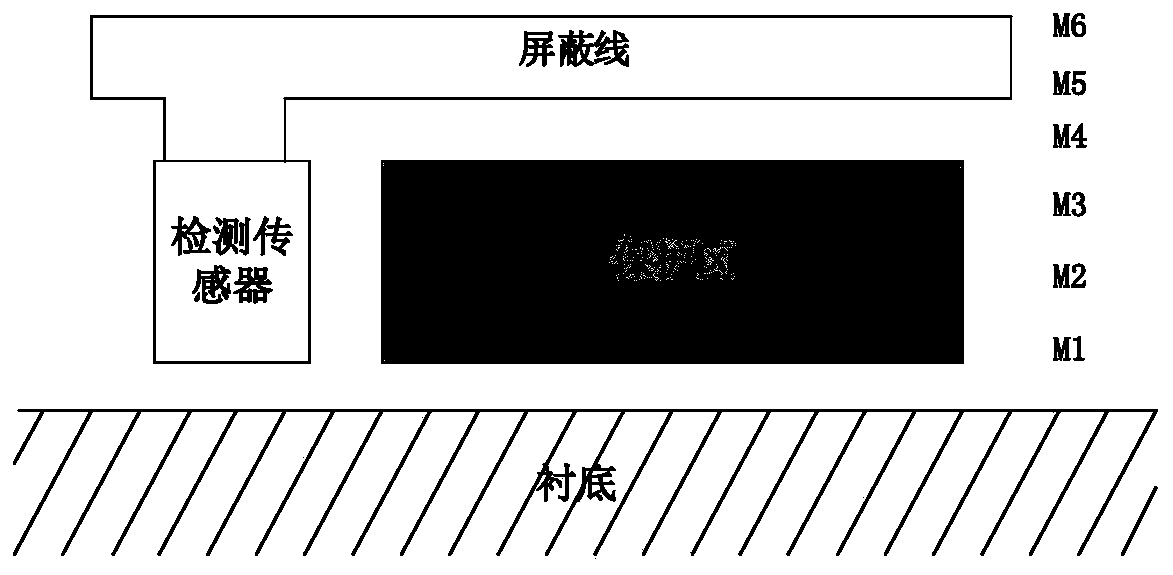
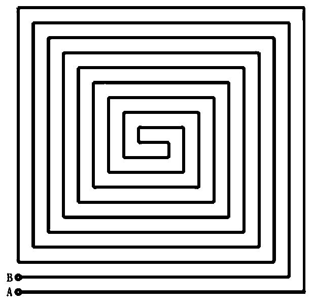
[0018] The present invention proposes a method for detecting the integrity of the top-layer metal protection layer based on a sigma-delta (Σ-Δ) modulator, the detection method is applicable to the top-layer metal protection layer of any graphic topological structure, and the present invention will take the spiral topological structure as the As an example, the integrity detection method is described. The spiral topology can be replaced by any other structure.

[0019] Such as figure 2 Shown is the wiring diagram of the top metal protection layer of the spiral topology. This protective layer is formed by metal wires AB. The metal line AB is composed of the top layer metal, and A and B are two ports respectively. The total resistance value of the metal wire AB is determined by its square resistance R, the width W of the metal wire, and the total length L of the metal wire. The total resistance value R AB =RL / W. Once the metal line AB is short-circuited from somewhere in th...


PUM


Abstract

The invention relates to the chip focusing resistance ion beam attack field and provides a top metal protection layer integrity detection method based on a sigma-delta modulator. In the method, through detecting whether a resistance value of a metal line is changed, whether a protection layer is complete is detected and then whether an attacker uses FIB to correct the protection layer is determined. A chip top protection layer integrity detection apparatus is formed by a top metal line AB, operation amplifiers AMP and AMP1, PMOS pipes M1 and M2, an NMOS pipe M3, switches S1 and S2, a reference current source I, a comparator COMP with a clock terminal, a counter CT and a digital comparator DCMP. The apparatus is mainly applied to a chip focusing resistance ion beam attack occasion.

Description

technical field [0001] The present invention relates to the field of chip anti-focused ion beam attack, and in particular to a chip top layer metal protection layer integrity detection structure based on a sigma-delta (Σ-Δ) modulator, specifically, a chip top layer protection layer integrity detection device and method. Background technique [0002] Focused Ion beam (FIB) attacks can deliberately cut integrated circuit chips or modify the original metal wiring, making the chip run wrong, or making some security protection modules lose their functions. The test nodes of the internal circuit can also be made through the FIB, and then the micro-probes can be used to directly monitor the test nodes and read the routing information. Therefore, FIB attacks seriously threaten the information security of integrated circuits. [0003] At present, the mainstream anti-attack method against FIB attacks is to use the top metal protection layer as the attack-aware structure. Such as f...

Claims


Application Information

Patent Timeline
Patent Type & Authority Patents(China)
IPC IPC(8): G01R31/28
CPCG01R31/2853
Inventor 赵毅强辛睿山王佳李跃辉
Owner TIANJIN UNIV
Why Eureka
Try Eureka