

Microdefect detection method, device and equipment for CF substrate
A technology for microscopic defects and detection methods, applied in the field of optical inspection, can solve the problems of unable to detect the shape, unable to reach the set threshold, affecting product quality, etc., to solve the problem of missing defects and improve the defect detection rate.
- Summary
- Abstract
- Description
- Claims
- Application Information
AI Technical Summary
Problems solved by technology
Method used
Image

Examples
Embodiment Construction
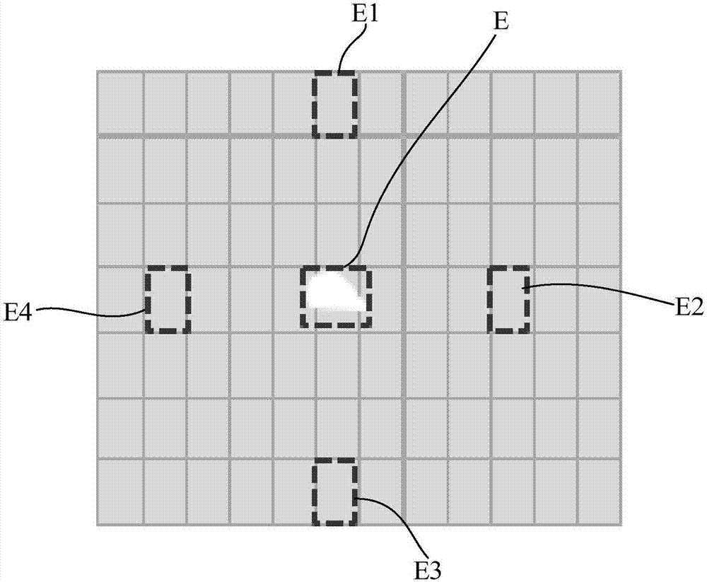
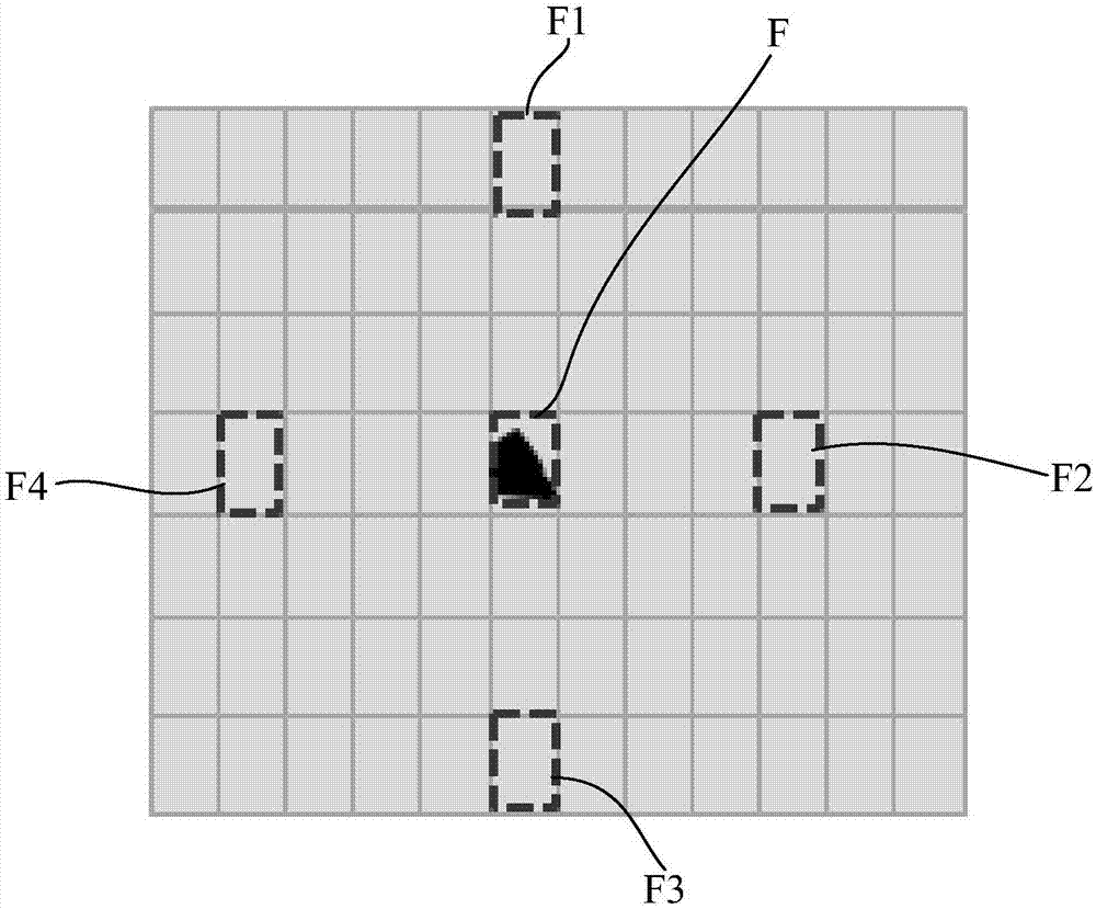
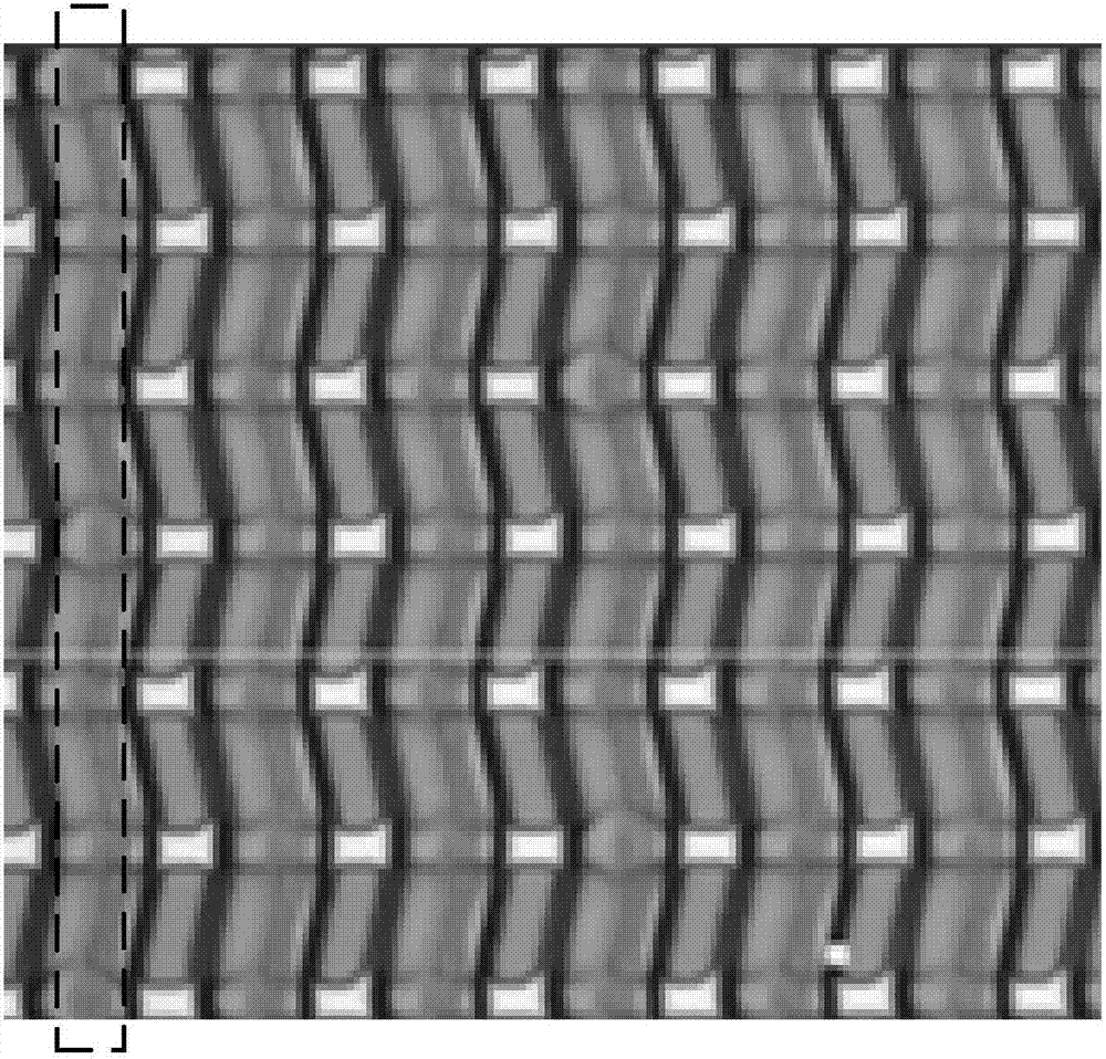
[0065] In order to better understand the above objects, features and advantages of the present invention, the present invention will be described in detail below in conjunction with the accompanying drawings and specific embodiments. It should be noted that, in the case of no conflict, the embodiments of the present application and the features in the embodiments can be combined with each other.
[0066] In the following description, a lot of specific details are set forth to facilitate a full understanding of the present invention, and the described embodiments are only some of the embodiments of the present invention, but not all of them. Based on the implementation manners in the present invention, all other implementation manners obtained by persons of ordinary skill in the art without making creative efforts belong to the scope of protection of the present invention.
[0067] Unless otherwise defined, all technical and scientific terms used herein have the same meaning as...
PUM
 Abstract
Description
Claims
Application Information