

Shift register and driving method thereof, light-emitting control circuit and display device
A shift register and node control technology, applied in static memory, digital memory information, instruments, etc., can solve the problems of increased process difficulty, shift register cannot be shifted and output normally, clock signal cannot be written, etc.
- Summary
- Abstract
- Description
- Claims
- Application Information
AI Technical Summary
Problems solved by technology
Method used
Image

Examples
Embodiment 1
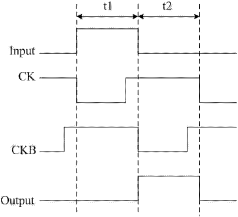
[0113] by Figure 5a The structure of the shift register shown is an example, the potential of the first reference signal terminal Vref1 is a high potential, and the potential of the second reference signal terminal Vref2 is a low potential. The corresponding input and output timing diagram is as follows Figure 7a As shown, specifically, the main selection is as Figure 7a In the shown input and output timing diagram, there are four stages: shift stage T1 , pull-up stage T2 , pull-down stage T3 and pull-down hold stage T4 .
[0114] In the shift stage T1, Input=1, CK1=0, CK2=1.
[0115] Since CK1=0, the first switching transistor M1 is turned on to provide the high-level signal of the input signal terminal Input to the first node N1, so that the first node N1 is at a high level. Since the first node N1 is at a high potential, both the third switch transistor M3 and the sixth switch transistor M6 are turned off, and the third capacitor C3 is charged. Since Input=1, the seco...
Embodiment 2
[0132] by Figure 5a The structure of the shift register shown is an example, the potential of the first reference signal terminal Vref1 is a high potential, and the potential of the second reference signal terminal Vref2 is a low potential. The corresponding input and output timing diagram is as follows Figure 7b As shown, specifically, an insertion stage T01 is inserted between the shift stage T1 and the pull-up stage T2 in the timing diagram of the first embodiment; wherein, the insertion stage T01 is further divided into a first insertion sub-stage T011 and a second insertion sub-stage T011 Stage T012.
[0133] In the shift stage T1, Input=1, CK1=0, CK2=1; and, after that, Input=1, CK1=1, CK2=1. The specific working process of this stage is basically the same as the working process of the shift stage T1 in the first embodiment, and will not be described in detail here.
[0134] In the first insertion sub-stage T011 of the insertion stage T01, Input=1, CK1=1, CK2=0.
[...
Embodiment 3
[0149] by Figure 5a The structure of the shift register shown is an example, the potential of the first reference signal terminal Vref1 is a high potential, and the potential of the second reference signal terminal Vref2 is a low potential. The corresponding input and output timing diagram is as follows Figure 7c As shown, specifically, two insertion stages T01 and T02 are inserted between the shift stage T1 and the pull-up stage T2 in the timing diagram of the first embodiment; wherein, the insertion stage T01 is further divided into a first insertion sub-stage T011 and the second insertion sub-stage T012; the insertion stage T02 is further divided into a first insertion sub-stage T021 and a second insertion sub-stage T022.
[0150] In the shift stage T1, Input=1, CK1=0, CK2=1; and, after that, Input=1, CK1=1, CK2=1. The specific working process of this stage is basically the same as the working process of the shift stage T1 in the first embodiment, and will not be describ...
PUM
 Abstract
Description
Claims
Application Information