Supercharge Your Innovation With Domain-Expert AI Agents!

Line edge roughness improvement with photon-assisted plasma process

A line edge roughness and plasma technology, applied in semiconductor/solid-state device manufacturing, discharge tubes, electrical components, etc.

Active Publication Date: 2017-12-19
LAM RES CORP
View PDF6 Cites 0 Cited by
  • Summary
  • Abstract
  • Description
  • Claims
  • Application Information

AI Technical Summary

Problems solved by technology

Let the process gas

Method used


Image

  • Line edge roughness improvement with photon-assisted plasma process
  • Line edge roughness improvement with photon-assisted plasma process
  • Line edge roughness improvement with photon-assisted plasma process

Examples


Embodiment

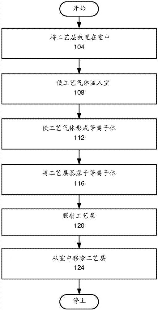
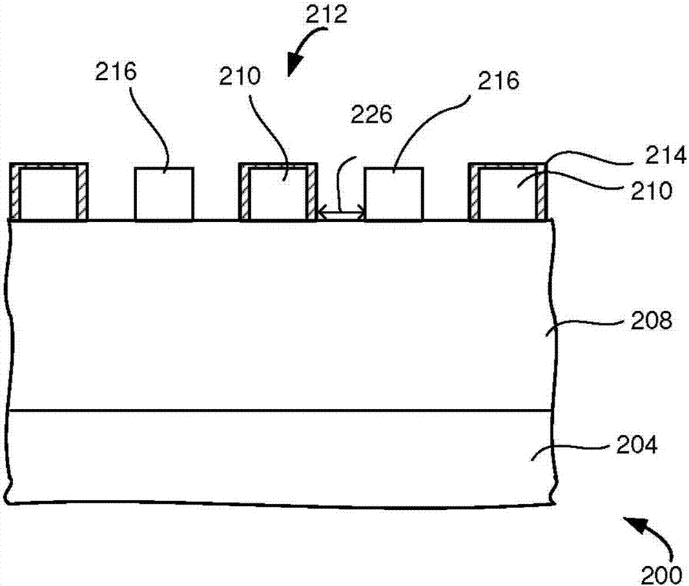
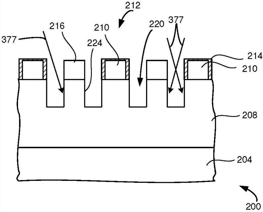
[0047] In a preferred embodiment, a substrate is provided having a silicon oxide-containing etch layer disposed beneath a double patterning mask. Double patterning masks are known in the art and include various processes for obtaining masks of higher resolution than a single mask patterning process can provide, enabling smaller devices and higher density. One example of a double patterning mask is described in Romano et al., US Patent No. 8,282,847, entitled "Photoresist Double Patterning," issued October 9, 2012, which is incorporated herein by reference for all purposes. The double patterning mask can be formed using self-aligned double patterning with spacer deposition. These processes are known in the art. An example of such a process is described in U.S. Patent No. 7,977,242 to Sadjadi et al., entitled "Double Mask Self-Aligned Patterning Technology (SADPT) Process," issued July 12, 2011, which is incorporated by reference in its entirety This article is for all purpos...


PUM


Abstract

A photon-assisted plasma processing method for processing a substrate with a process layer is provided. A process gas is flowed into the chamber. The process gas is formed into a plasma. The process layer is exposed to the plasma. The process layer is illuminated with a light with a wavelength of between 200 nm and 1 micron, while exposing the substrate to the plasma.

Description

technical field [0001] The present invention relates to methods of forming semiconductor devices on semiconductor wafers. More specifically, the present disclosure relates to etching layers in the formation of semiconductor devices. Background technique [0002] In forming a semiconductor device, the etch layer may be etched. Contents of the invention [0003] To achieve the above object, and in accordance with the object of the present disclosure, a photon-assisted plasma processing method for improving line edge roughness or line width roughness of a substrate having a process layer is provided. Process gas is flowed into the chamber. The process gas forms a plasma. The process layer is exposed to the plasma. The process layer is irradiated with light having a wavelength between 200 nm and 1 micron while exposing the substrate to the plasma. [0004] In another expression, an apparatus for processing a substrate is provided. A substrate support for supporting the s...

Claims


Application Information

Patent Timeline
IPC IPC(8): H01L21/67H01J37/32
CPCH01J37/321H01J37/32137H01L21/67069H01J2237/3341H01J2237/327H01L21/31116H01L21/31144H01J37/32082H01J37/3244H01L21/3065H01L21/02021H01L21/02315
Inventor 谭忠魁徐晴傅乾桑军·帕克
Owner LAM RES CORP
Features
  • R&D
  • Intellectual Property
  • Life Sciences
  • Materials
  • Tech Scout
  • Unparalleled Data Quality
  • Higher Quality Content
  • 60% Fewer Hallucinations
Learn More