Supercharge Your Innovation With Domain-Expert AI Agents!

Device for cutting silicon wafers

A silicon wafer cutting and cutting mechanism technology, applied in fine working devices, stone processing equipment, manufacturing tools, etc., can solve the problems of high production cost, waste, and low cutting work efficiency, and achieve strong practicability and avoid cutting failures. Accurate effect

Inactive Publication Date: 2018-01-05
安徽中柜智能科技有限公司
View PDF6 Cites 2 Cited by
  • Summary
  • Abstract
  • Description
  • Claims
  • Application Information

AI Technical Summary

Problems solved by technology

Among them, slicing is the process of cutting silicon rods into silicon wafers. In the cutting process, if the cutting is not accurate, there will be deviation during cutting, which will lead to low cutting efficiency, resulting in unnecessary waste and production. High cost; and in the existing cutting device, the same device can only cut silicon wafers of one size, if you want to cut silicon wafers of another size, you must change a cutting device, so the cost is relatively high high

Method used


Image

  • Device for cutting silicon wafers
  • Device for cutting silicon wafers

Examples


Embodiment Construction

[0014] In order to have a further understanding and understanding of the structural features of the present invention and the achieved effects, the preferred embodiments and accompanying drawings are used for a detailed description, as follows:

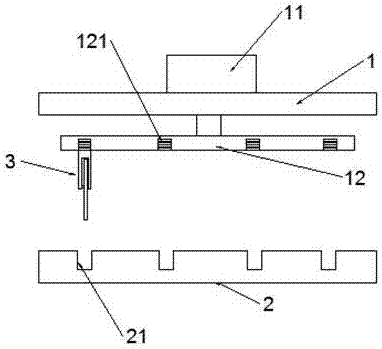
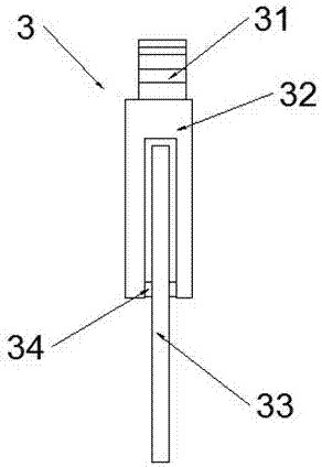
[0015] as attached Figure 1~2 As shown, a device for cutting silicon wafers includes a beam 1, a base 2, a cutting mechanism 3, and a push plate 12; the beam 1 is located directly above the base 2, and the push plate 12 is arranged on the beam 1 and the base 2;

[0016] A cylinder 11 is arranged in the middle of the top of the crossbeam 1, the telescoping end of the cylinder 11 is arranged at the bottom of the crossbeam 1, and the push plate 12 is horizontally arranged on the telescoping end of the cylinder 11 near the end of the base 2; The push plate 12 is longitudinally provided with several fixing holes 121; the base 2 is provided with several cutting grooves 21; the cutting grooves 21 correspond to the fixing holes 121 one by o...


PUM


Abstract

The invention discloses a device for cutting silicon wafers. The device for cutting the silicon wafers comprises a cross beam, a base, cutting mechanisms and a push plate, wherein the cross beam is located right above the base, and the push plate is arranged between the cross beam and the base. The device for cutting the silicon wafers has the following beneficial effects: (1), cutting grooves inthe base have a positioning function so that cutting inaccuracy caused by deviation during cutting can be avoided; and (2), fibolts are in threaded connection with fixing holes, so that a distance between the two cutting mechanisms is adjusted according to size requirements, and practicability is high.

Description

technical field [0001] The invention belongs to the technical field of solar battery sheet preparation, and in particular relates to a device for cutting silicon wafers. Background technique [0002] The process flow of solar panel production is slicing→cleaning→preparing suede→peripheral etching→removing the PN+ junction on the back→making upper and lower electrodes→making anti-reflection film→sintering→testing→grading. Among them, slicing is the process of cutting silicon rods into silicon wafers. In the cutting process, if the cutting is not accurate, there will be deviation during cutting, which will lead to low cutting efficiency, resulting in unnecessary waste and production. High cost; and in the existing cutting device, the same device can only cut silicon wafers of one size, if you want to cut silicon wafers of another size, you must change a cutting device, so the cost is relatively high high. Contents of the invention [0003] The object of the present inventi...

Claims


Application Information

Patent Timeline
Patent Type & Authority Applications(China)
IPC IPC(8): B28D5/00
Inventor 孙文生孙传涛
Owner 安徽中柜智能科技有限公司
Features
  • R&D
  • Intellectual Property
  • Life Sciences
  • Materials
  • Tech Scout
  • Unparalleled Data Quality
  • Higher Quality Content
  • 60% Fewer Hallucinations
Learn More