

Device and method for detecting surface defects of planar optical element
A technology of optical components and detection devices, applied in the direction of optical testing defects/defects, etc., can solve the problems of inability to provide defects, affecting imaging quality, energy loss, etc., and achieve the effect of improving detection efficiency and detection accuracy
- Summary
- Abstract
- Description
- Claims
- Application Information
AI Technical Summary
Problems solved by technology
Method used
Image


Examples
Embodiment Construction
[0019] In order to make the object, technical solution and advantages of the present invention clearer, the present invention will be further described in detail below in conjunction with the accompanying drawings and specific embodiments. It should be understood that the specific embodiments described here are only used to explain the present invention, but not to limit the present invention.
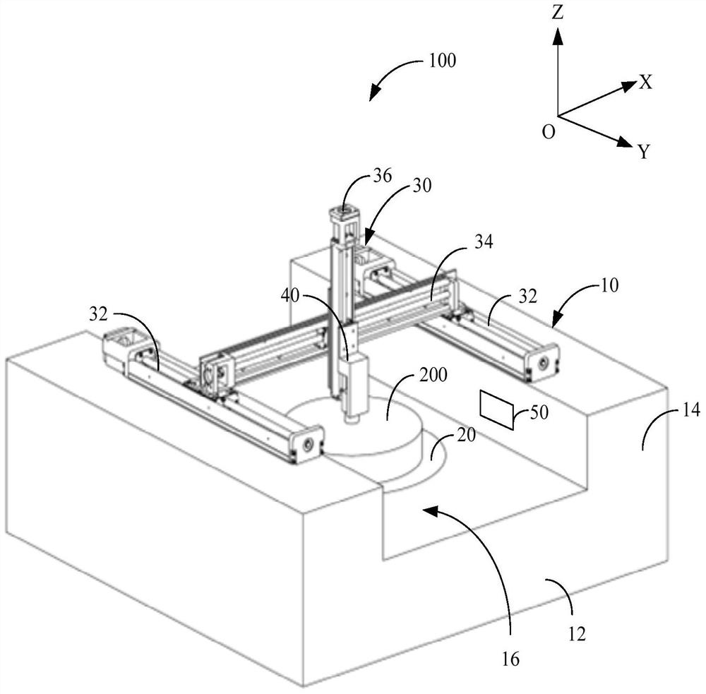
[0020] see Figure 1 to Figure 3 , is a structural schematic diagram of a detection device for surface defects of optical components. The detection device 100 includes a workbench 10 . The workbench 10 includes a support body 12 and a support column 14 disposed on the support body 12 . In this embodiment, the number of the support columns 14 is two, and the two support columns 14 are arranged on both sides of the support body 12, and the support body 12 and the two support columns 14 form a The receiving space 16 is roughly U-shaped.
[0021] The detection device 100 also includes ...
PUM
 Abstract
Description
Claims
Application Information