Array substrate, display panel and display device

An array substrate and substrate technology, applied in optics, instruments, electrical digital data processing, etc., can solve the problems of unfavorable display device narrow frame, affect the performance of pressure sensor, unfavorable heat dissipation of pressure sensor, etc., so as to facilitate heat dissipation and prolong use The effect of improving life and performance

Inactive Publication Date: 2018-01-09
XIAMEN TIANMA MICRO ELECTRONICS
View PDF5 Cites 10 Cited by
  • Summary
  • Abstract
  • Description
  • Claims
  • Application Information

AI Technical Summary

Problems solved by technology

[0003] In the prior art, the pressure sensor is arranged in the non-display area of ​​the display device. Since the non-display area is located in the frame area of ​​the display device, and since the size of the pressure sensor is large (generally 120um*120um), if the size is larger The pressure sensor is set in the non-display area. In order to have space to set the pressure sensor, it is necessary to make the frame area of ​​the display device wider, which is not conducive to the narrow frame of the display device.
Moreover, the pressure sensor is generally composed of multiple strain pressure sensors that are electrically connected. When the pressure sensor is placed in the non-display area, the multiple strain pressure sensors need to be integrated, which is not conducive to the heat dissipation of the pressure sensor, thereby affecting the performance of the pressure sensor. , if the temperature is high, it is easy to cause damage to the pressure sensor

Method used


Image

  • Array substrate, display panel and display device
  • Array substrate, display panel and display device
  • Array substrate, display panel and display device

Examples


Embodiment Construction

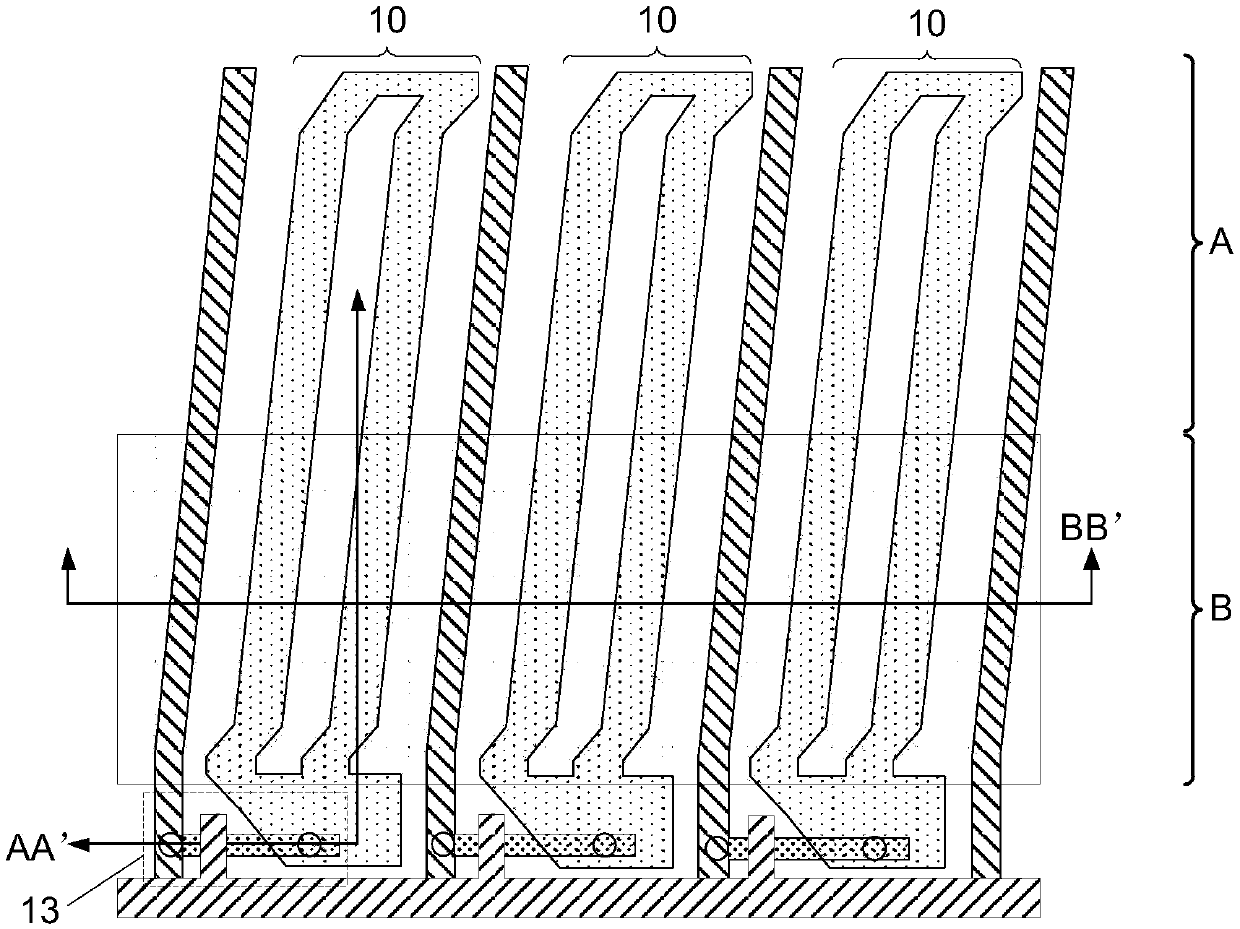
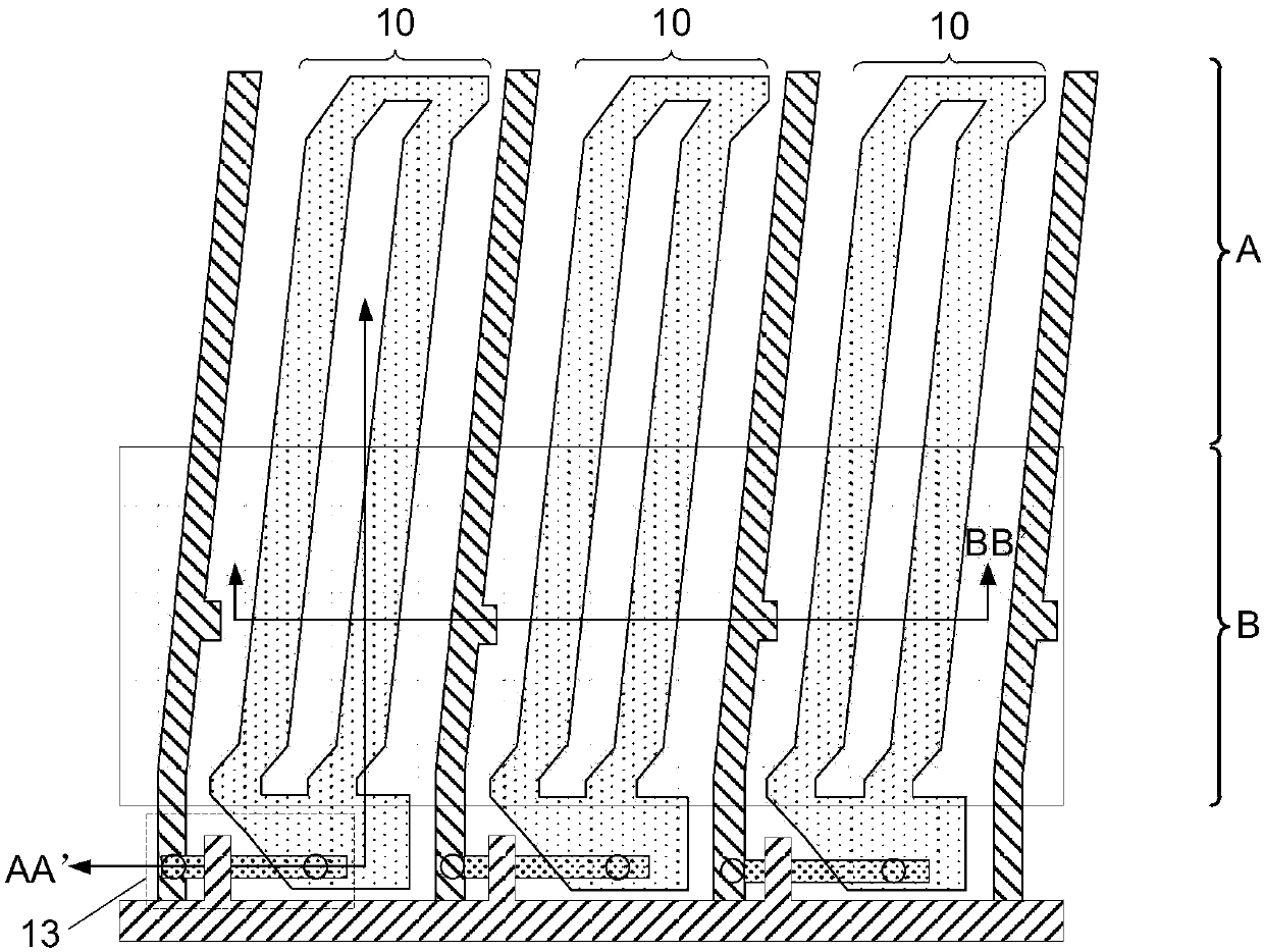
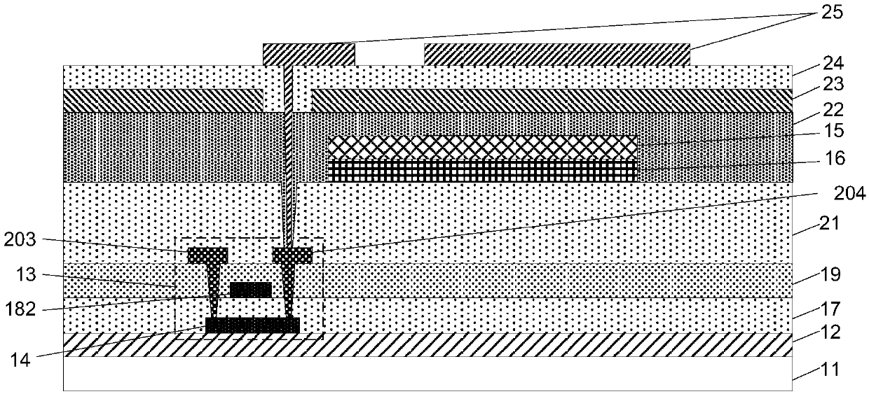
[0065] In order to make the purpose, technical solutions and advantages of the embodiments of the present invention clearer, the technical solutions in the embodiments of the present invention will be clearly and completely described below in conjunction with the drawings in the embodiments of the present invention. Obviously, the described embodiments It is a part of embodiments of the present invention, but not all embodiments. Based on the embodiments of the present invention, all other embodiments obtained by persons of ordinary skill in the art without creative efforts fall within the protection scope of the present invention.

[0066] Terms used in the embodiments of the present invention are only for the purpose of describing specific embodiments, and are not intended to limit the present invention. As used in the embodiments of the present invention and the appended claims, the singular forms "a", "said" and "the" are also intended to include the plural forms unless th...


PUM


Abstract

An embodiment of the invention relates to the technical field of display and provides an array substrate, a display panel and a display device. The array substrate comprises a display area and a non-display area surrounding the display area, and the display area comprises a plurality of sub-pixels. Each sub-pixel comprises a substrate, a buffer layer and a thin film transistor array, wherein the buffer layer is arranged above the substrate, and the thin film transistor array is arranged on one side, away from the substrate, of the buffer layer and comprises an active layer. Each sub-pixel comprises a transmission area and a reflection area, wherein the reflection area comprises a reflection electrode arranged on one side, away from the corresponding substrate, of the corresponding thin film transistor array. The reflection areas of part of the sub-pixels further comprise pressure sensors, and each pressure sensor is arranged between the corresponding reflection electrode and the corresponding buffer layer. By adoption of the technical scheme, convenience in realization of a narrow bezel of the display device is achieved, and heat radiation performances of the pressure sensors are improved.

Description

technical field [0001] The present invention relates to the field of display technology, in particular to an array substrate, a display panel and a display device. Background technique [0002] With the rapid development of display technology, users have higher and higher demands on the performance of display devices, and display panels with touch functions emerge as the times require. In order to provide multiple human-computer interaction methods and multiple touch functions, the display device generally has a touch sensor (Touch Sensor) and a force sensor (Force Sensor). The touch sensor is mainly used to detect the pressing position and whether there is a pressing operation. The sensor is mainly used to detect the pressure when pressing. [0003] In the prior art, the pressure sensor is arranged in the non-display area of ​​the display device. Since the non-display area is located in the frame area of ​​the display device, and since the size of the pressure sensor is la...

Claims


Application Information

Patent Timeline
Patent Type & Authority Applications(China)
IPC IPC(8): G02F1/1333G02F1/1368G02F1/1343G06F3/041
Inventor 宋琼郑斌义吴玲沈柏平
Owner XIAMEN TIANMA MICRO ELECTRONICS
Why Eureka
Try Eureka