
Display panel and display device applied to it

A display panel and display area technology, applied to static indicators, instruments, etc., can solve problems such as different charging capabilities of gate-on-chip films, poor horizontal blocks, and reduced panel image quality, and improve pixel brightness. problems, improve display uniformity, and avoid charging unevenness

Active Publication Date: 2018-01-19
HKC CORP LTD +1
View PDF5 Cites 10 Cited by
  • Summary
  • Abstract
  • Description
  • Claims
  • Application Information

AI Technical Summary

Problems solved by technology

[0004] However, when TFT-LCD panels are displayed, due to lack of design, there will often be severe uneven brightness distribution on the screen, which will affect the overall display effect of the panel, which is the so-called H-block phenomenon (Horizontal Block, poor horizontal block)
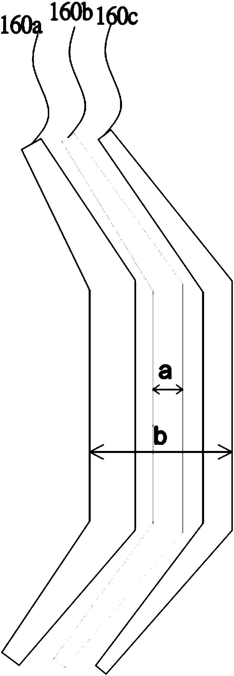
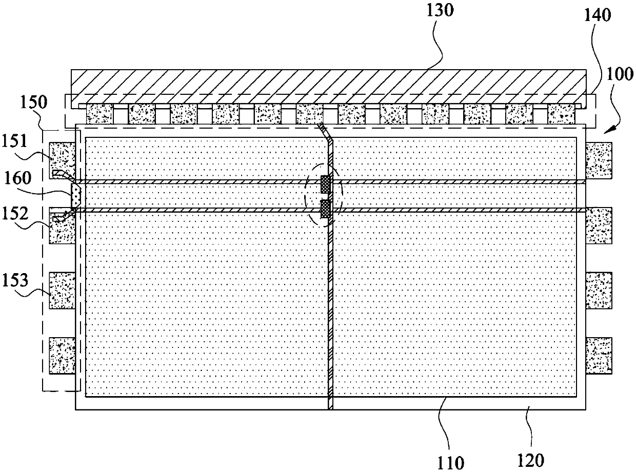
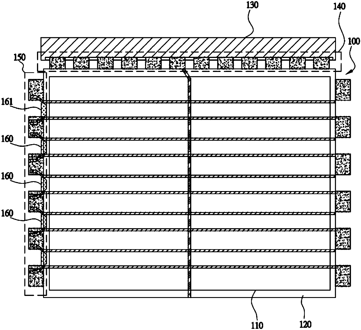
This H-block occurs between gate-on-chip films (Gate COF), due to the impedance of the array wiring (Wire On Array, WOA) between gate-on-chip films (Gate to Gate, G-G), and the array The longer the wiring (Wire On Array, WOA), the greater the corresponding impedance value, resulting in different charging capabilities of the gate chip-on-chip film corresponding to each block
Even if the adjacent gate-on-chip films are connected to each other, the charging conditions of the pixel units connected to them are inconsistent, which makes the panel brightness difference very obvious and the panel image quality is reduced.

Method used


Image

  • Display panel and display device applied to it
  • Display panel and display device applied to it
  • Display panel and display device applied to it

Examples


Embodiment Construction

[0028] The following descriptions of the various embodiments refer to the accompanying drawings to illustrate specific embodiments in which the present invention can be practiced. The directional terms mentioned in the present invention, such as "up", "down", "front", "back", "left", "right", "inside", "outside", "side", etc., are for reference only The orientation of the attached schema. Therefore, the directional terms used are used to illustrate and understand the present invention, but not to limit the present invention.

[0029] The drawings and descriptions are to be regarded as illustrative in nature and not restrictive. In the figures, structurally similar units are denoted by the same reference numerals. In addition, the size and thickness of each component shown in the drawings are arbitrarily shown for understanding and ease of description, but the present invention is not limited thereto.

[0030] In the drawings, the thickness of layers, films, panels, regions,...


PUM


Abstract

The invention discloses a display panel and display device applied to it. The display panel comprises a substrate, multiple grid crystal covering films, and a transmission line; the substrate comprises a display zone and a wiring zone at the periphery thereof, and the display zone is provided with multiple active switches and multiple pixel units; the multiple grid crystal covering films are laminated on the edge of the substrate and located in the wiring zone; the transmission zone comprises multiple driving line sections, arranged between multiple grid crystal covering films and electricallyconnected with multiple grid crystal covering films, wherein a first driving line section is arranged between adjacent first crystal covering film and a second crystal covering film in multiple gridcrystal covering films; the line width of the first driving line section is more than that of the other multiple driving line sections. According to the driving line width between previous two grid crystal covering films in a driving signal order obtained through adjustment, charging ability of the grid crystal covering film in the place is changed; the difference of pixel brightness between the zone and the other zone is reduced, and the display homogeneity of the liquid crystal panel is improved.

Description

technical field [0001] The invention relates to the field of display technology, in particular to a display panel and a display device for its application. Background technique [0002] When the TFT-LCD (active switch-liquid crystal display) panel is displayed normally, it is necessary to combine the gate driver circuit (GateDriver) with the gate line (Gate line), the source driver circuit (Source) with the data line (Data line), and the color filter The common electrode of the light sheet substrate (color filter common electrode, CF com) and the storage electrode. Wherein the signal of the pixel (pixel) electrode is supplied by the data line after the active switch (TFT) is turned on. The storage electrode signal is supplied by the array sharing line (AACom) on the periphery of the effective display area to form a storage capacitor (Cst) with the pixel electrode. The common electrode signal of the color filter is supplied to the color filter substrate by the common voltag...

Claims


Application Information

Patent Timeline
Patent Type & Authority Applications(China)
IPC IPC(8): G02F1/133G09G3/36
Inventor 杨艳娜
Owner HKC CORP LTD
Learn More