Electron transport layer inkjet printing ink and preparation method thereof

An electron transport layer and inkjet printing technology, applied in the direction of inks, circuits, electrical components, etc., can solve the problems of easy miscibility, high cost, and high production cost of OLED devices, and achieve the effect of avoiding miscibility and meeting the requirements of the process

Active Publication Date: 2020-06-26
SHENZHEN CHINA STAR OPTOELECTRONICS SEMICON DISPLAY TECH CO LTD
View PDF9 Cites 0 Cited by
  • Summary
  • Abstract
  • Description
  • Claims
  • Application Information

AI Technical Summary

Problems solved by technology

[0005] At present, the most commonly used preparation methods for OLED devices are: the hole injection layer, the hole transport layer and the light-emitting layer are prepared by ink-jet printing (Ink-Jet Printing), and the electron transport layer and cathode are prepared by vacuum thermal evaporation. The cost of thermal evaporation method is high, resulting in high production cost of OLED devices, which limits the large-scale commercialization of OLED devices
The inkjet printing method uses multiple nozzles to drop functional material ink into a predetermined pixel area, and then obtains the desired film by drying. This method has the advantages of high material utilization and is a key technology to solve the cost problem of large-scale OLED display. However, , due to the mutual dissolution phenomenon between adjacent printing ink layers, and the materials of the electron transport layer and the cathode are mostly evaporated materials, it is difficult to realize the OLED device of the full solution process.
[0006] Conjugated cationic electrolyte is a kind of soluble electron transport material, which has been proved to have excellent electron transport characteristics in OLED and OPV (organic solar cell) devices, which can significantly improve device performance; therefore, the ionic conjugated polyelectrolyte Dispersed in a solvent to prepare an inkjet printing ink for the electron transport layer, and use methods such as printing, pad printing, and spin coating to prepare the electron transport layer, which is conducive to the production of full-solution OLED devices, but the inkjet printing equipment and printing process are harmful to the ink. There are certain requirements. In order to make the ink suitable for inkjet printing technology, it is usually necessary to comprehensively adjust the solvent components, viscosity and surface tension of the ink, so it is suitable for inkjet inkjet of the electron transport layer of inkjet printing equipment and printing process conditions Printing ink needs to be improved

Method used


Image

  • Electron transport layer inkjet printing ink and preparation method thereof

Examples


Embodiment Construction

[0028] In order to further illustrate the technical means adopted by the present invention and its effects, the following describes in detail in conjunction with preferred embodiments of the present invention and accompanying drawings.

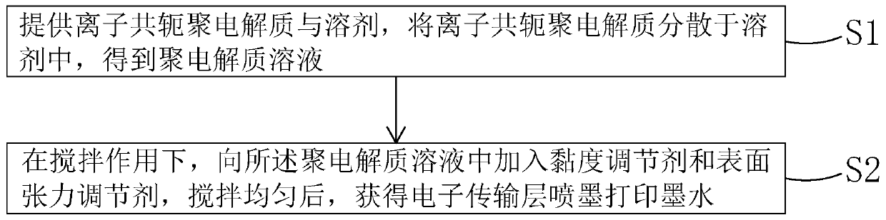
[0029] see figure 1 , the present invention provides a kind of preparation method of electron transport layer ink-jet printing ink, comprises the steps:

[0030] Step 1, providing an ionic conjugated polyelectrolyte and a solvent, and dispersing the ionic conjugated polyelectrolyte in the solvent to obtain a polyelectrolyte solution.

[0031] Specifically, the ionic conjugated polyelectrolyte may be a cationic conjugated polyelectrolyte or an anionic conjugated polyelectrolyte, preferably a cationic conjugated polyelectrolyte.

[0032] Preferably, the cationic conjugated polyelectrolyte is a carboxyl-substituted cationic conjugated polyelectrolyte.

[0033] Preferably, the metal cation in the cationic conjugated polyelectrolyte is a sodium i...


PUM

PropertyMeasurementUnit
boiling pointaaaaaaaaaa

Abstract

The invention provides an electron transport layer inkjet printing ink and a preparation method thereof. The preparation method of inkjet printing ink for electron transport layer of the present invention adopts ionic conjugated polyelectrolyte as solute, alcohol compound as solvent, and obtains an electronic ink suitable for inkjet printing technology by adjusting the proportion, viscosity and surface tension of each component. The inkjet printing ink for the transport layer, the inkjet printing ink for the electron transport layer can meet the process requirements of inkjet printing, realize the inkjet printing method of the electron transport layer, and can avoid the electron transport layer and the adjacent structural layer in the OLED preparation process. The phenomenon of mutual dissolution occurs between them, which is conducive to the realization of the production of all-solution OLED devices. The electron transport layer inkjet printing ink of the present invention is prepared by the above method, can meet the process requirements of inkjet printing, realize the inkjet printing method of the electron transport layer, and is beneficial to realize the production of full solution OLED devices.

Description

technical field [0001] The invention relates to the field of display technology, in particular to an electron transport layer inkjet printing ink and a preparation method thereof. Background technique [0002] Organic Light Emitting Display (OLED) has self-illumination, low driving voltage, high luminous efficiency, short response time, high definition and contrast, nearly 180° viewing angle, wide operating temperature range, and can realize flexible display and With many advantages such as large-area full-color display, it is recognized by the industry as a display device with the most potential for development. [0003] According to the driving method, OLED can be divided into two categories: passive matrix OLED (Passive Matrix OLED, PMOLED) and active matrix OLED (Active Matrix OLED, AMOLED), namely direct addressing and thin film transistor matrix addressing. Among them, AMOLED has pixels arranged in an array, belongs to the active display type, has high luminous effici...

Claims


Application Information

Patent Timeline
Patent Type & Authority Patents(China)
IPC IPC(8): H01L51/56H01L51/50
CPCH10K50/16H10K71/00C09D11/38C09D11/52C09D11/36H10K71/135H10K71/15C09D11/30H10K50/17
Inventor 史婷
Owner SHENZHEN CHINA STAR OPTOELECTRONICS SEMICON DISPLAY TECH CO LTD
Why Eureka
Try Eureka