Array substrate manufacturing method, array substrate and display panel

A technology of an array substrate and a manufacturing method, applied in the display field, can solve the problem of a large peripheral area of ​​a display panel, and achieve the effect of less width

Active Publication Date: 2018-02-23
BOE TECH GRP CO LTD +1
View PDF2 Cites 17 Cited by
  • Summary
  • Abstract
  • Description
  • Claims
  • Application Information

AI Technical Summary

Problems solved by technology

[0005] Embodiments of the present invention provide a method for manufacturing an array substrate, an array substrate, and a display panel, so as to solve the problem that a sufficient area needs to be reserved on the display panel for wiring bonding, resulting in a large peripheral area of ​​the display panel.

Method used


Image

  • Array substrate manufacturing method, array substrate and display panel
  • Array substrate manufacturing method, array substrate and display panel
  • Array substrate manufacturing method, array substrate and display panel

Examples


Embodiment Construction

[0019] The following will clearly and completely describe the technical solutions in the embodiments of the present invention with reference to the accompanying drawings in the embodiments of the present invention. Obviously, the described embodiments are some of the embodiments of the present invention, but not all of them. Based on the embodiments of the present invention, all other embodiments obtained by persons of ordinary skill in the art without creative efforts fall within the protection scope of the present invention.

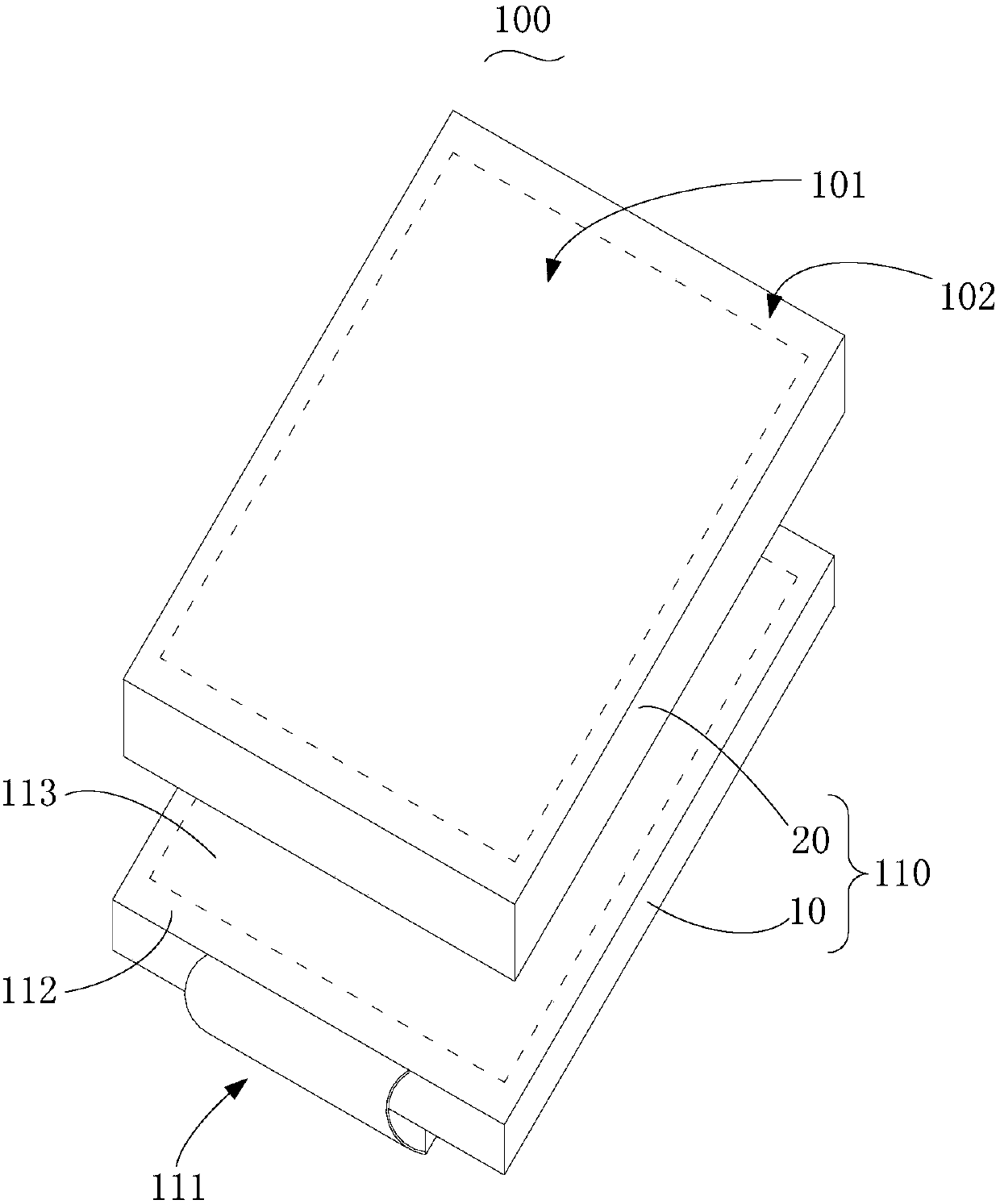
[0020] see figure 1 , figure 1 A perspective view of a display device provided by a preferred embodiment of the present invention. Such as figure 1 As shown, the display device 100 includes a display panel 110, the display panel 110 includes an array substrate 10 and an opposite substrate 20, the array substrate 10 is arranged opposite to the opposite substrate 20, and the array substrate 10 and the A liquid crystal layer (not shown) is interposed b...


PUM


Abstract

The invention provides an array substrate manufacturing method, an array substrate and a display panel. A removal area and a reserve area are arranged in a bending area in a peripheral area of a substrate, a substrate positioned in the middle removal area is removed, a routing layer positioned in the removal area is bent, a substrate in the reserve area is parallel and opposite to the substrate inthe peripheral area, the width of the peripheral area of one end for binding lines of the array substrate can be effectively decreased, and narrow bezel of the display panel and a display device is benefited.

Description

technical field [0001] The present invention relates to the field of display technology, in particular to a method for manufacturing an array substrate, an array substrate and a display panel. Background technique [0002] The demand for various display devices has increased with the rise of the global information society. Therefore, great efforts have been devoted to the research and development of various flat display devices such as liquid crystal display devices (LCD), plasma display devices (PDP), electroluminescent display devices (ELD), and vacuum fluorescent display devices (VFD). . [0003] With the popularization of display devices, users not only have higher and higher requirements for the functions and performance of display devices, but also have higher and higher requirements for the appearance of display devices. And other conditions are also increasingly becoming factors for selecting a display device. [0004] However, in existing display devices, since v...

Claims


Application Information

Patent Timeline
Patent Type & Authority Applications(China)
IPC IPC(8): G02F1/13G02F1/1333
CPCG02F1/1303G02F1/1333G02F1/133302G02F1/133388
Inventor 冯彬峰
Owner BOE TECH GRP CO LTD
Why Eureka
Try Eureka