Touch display substrate and touch display device

A technology for touch display substrates and touch display devices, which is applied to static indicators, instruments, calculations, etc., can solve the problems of uneven distribution of touch electrode lines and poor display uniformity of touch display devices, and achieve improved display performance. Uniformity, improve the effect of uneven distribution

Active Publication Date: 2018-02-27
HEFEI BOE OPTOELECTRONICS TECH +1
View PDF7 Cites 5 Cited by
  • Summary
  • Abstract
  • Description
  • Claims
  • Application Information

AI Technical Summary

Problems solved by technology

[0003] In view of this, the present invention provides a touch display substrate and a touch display device, which are used to solve the proble

Method used


Image

  • Touch display substrate and touch display device
  • Touch display substrate and touch display device
  • Touch display substrate and touch display device

Examples


Embodiment 1

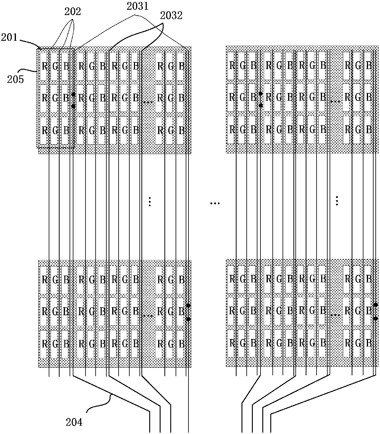
[0043] Please refer to figure 1 , figure 1 It is a schematic diagram of a touch display substrate according to Embodiment 1 of the present invention. The touch display substrate includes a base substrate (not shown in the figure), and the base substrate includes a display area and a lead area. A touch electrode 201, a plurality of wires, a plurality of data lines 202, and a plurality of pixel units.

[0044] The wiring and the data wiring 202 are arranged in the same layer and material in parallel, and each of the touch electrodes 201 is provided with a plurality of wiring in the orthographic projection area of ​​the base substrate, and each of the touch electrodes 201 is provided with a plurality of wiring The multiple wires corresponding to the electrodes 201 include a touch electrode wire 2031 for connecting to the touch electrode 201 and multiple auxiliary wires 2032 not connected to the touch electrode 201 . A plurality of lead wires 204 are arranged in the lead wire ar...

Embodiment 2

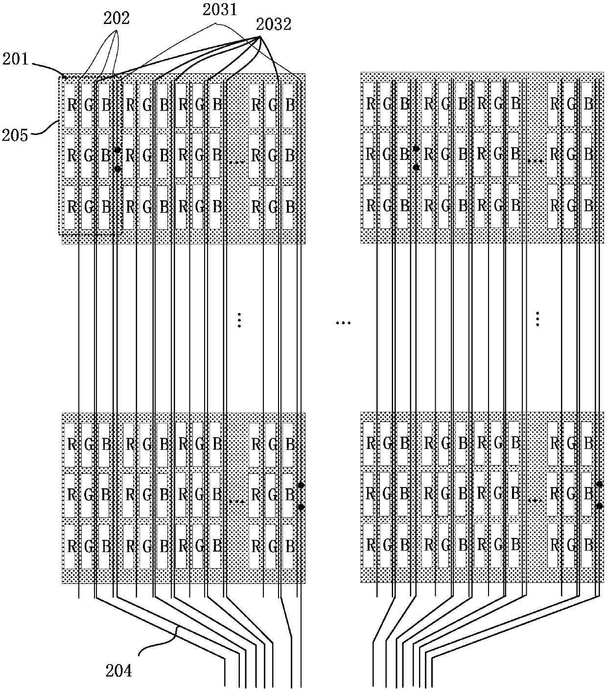
[0048] Please refer to figure 2 , figure 2 It is a schematic diagram of a touch display substrate according to Embodiment 2 of the present invention. The touch display substrate includes a base substrate (not shown in the figure), and the base substrate includes a display area and a lead area. A touch electrode 201, a plurality of wires, a plurality of data lines 202 and a plurality of pixel units.

[0049] The wiring and the data wiring 202 are arranged in the same layer and material in parallel, and each of the touch electrodes 201 is provided with a plurality of wiring in the orthographic projection area of ​​the base substrate, and each of the touch electrodes 201 is provided with a plurality of wiring The multiple wires corresponding to the electrodes 201 include a touch electrode wire 2031 for connecting with the corresponding touch electrode 201 and multiple auxiliary wires 2032 not connected with the touch electrode. A plurality of lead wires 204 are arranged in th...

Embodiment 3

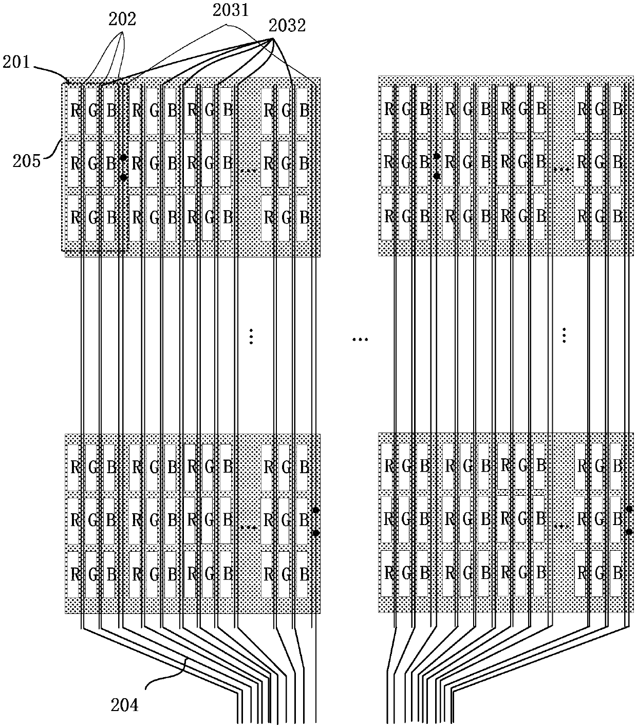
[0053] Please refer to image 3 , image 3 It is a schematic diagram of a touch display substrate according to Embodiment 3 of the present invention. The touch display substrate includes a base substrate (not shown in the figure), and the base substrate includes a display area and a lead area. A touch electrode 201, a plurality of wires, a plurality of data lines 202 and a plurality of pixel units.

[0054] The wiring and the data wiring 202 are arranged in the same layer and in parallel, and each of the touch electrodes 201 is provided with a plurality of wiring in the orthographic projection area of ​​the base substrate, and each of the touch electrodes 201 The corresponding multiple wires include a touch electrode wire 2031 for connecting with the corresponding touch electrode 201 and multiple auxiliary wires 2032 not connected with the touch electrode. A plurality of lead wires 204 are arranged in the lead wire area, and the wires are connected to the lead wires 204 in o...


PUM


Abstract

The invention provides a touch display substrate and a touch display device. The touch display substrate comprises an underlayer substrate which comprises a display area and a lead area, multiple touch electrodes and multiple wires are arranged in the display area, the wires comprise touch electrode wires used for being connected with the touch electrodes and auxiliary wires which are not connected with the touch electrodes, at least two wires are arranged in an orthographic projection area of each touch electrode on the underlayer substrate, multiple leads are arranged in the lead area, and each wire is connected with a touch signal output end of a driving circuit through the corresponding lead. Accordingly, at least two wires are arranged in the orthographic projection area of each touchelectrode on the underlayer substrate, and then the at least two wires can be distributed in the area where the touch electrodes are located as uniform as possible, the problem that the touch electrode wire distribution is nonuniform is solved, and the display uniformity of the touch display device containing the touch display substrate is improved.

Description

technical field [0001] The present invention relates to the field of display technology, in particular to a touch display substrate and a touch display device. Background technique [0002] In the existing design of self-contained in-cell touch display devices, the touch electrodes are usually in the form of blocks, which are multiplexed with the common electrodes, and the touch electrodes are connected to the touch control circuit of the driving circuit through the touch electrode traces. The signal output terminal is connected, and each touch electrode corresponds to a touch electrode wiring connected thereto. During the display period, the drive circuit inputs a common voltage signal to the touch electrodes through the touch electrode wiring, and inputs a touch signal to the touch electrodes through the touch electrode wiring during the touch period. There are multiple pixel units (pixels) in the area where the touch electrodes are located. One pixel unit includes three ...

Claims


Application Information

Patent Timeline
IPC IPC(8): G06F3/041
CPCG06F3/0412G09G3/20G06F3/0443G06F3/04164G09G2300/0426G09G2354/00G06F3/047G06F3/044G09G2310/0264G06F2203/04112
Inventor 刘波邵贤杰古宏刚
Owner HEFEI BOE OPTOELECTRONICS TECH
Why Eureka
Try Eureka