Semiconductor device, display apparatus, method of manufacturing semiconductor device and method of manufacturing display apparatus
A technology of semiconductors and oxide semiconductors, applied in semiconductor/solid-state device manufacturing, semiconductor devices, static indicators, etc., can solve problems such as the decline in productivity of semiconductor devices, and achieve the effect of suppressing the decline in productivity
- Summary
- Abstract
- Description
- Claims
- Application Information
AI Technical Summary
Problems solved by technology
Method used
Image
Examples
Embodiment approach 1
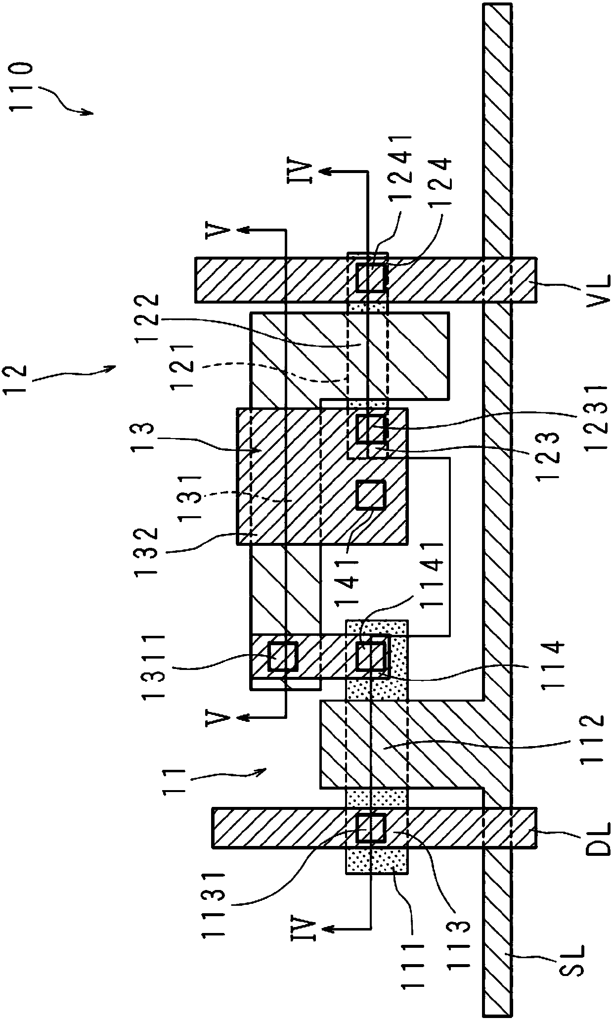
[0052] image 3 It is a plan view showing a structural example of the semiconductor device 10 included in the pixel drive circuit. Figure 4 Is along image 3 A cross-sectional view taken along the section line IV-IV in. The semiconductor device 110 includes an insulating substrate 101, a polysilicon layer 111, a first gate insulating layer 102, a first metal layer 103, an oxide semiconductor layer 121, a second gate insulating layer 104, a second metal layer 105, and an interlayer insulating layer 106 and the third metal layer 107.
[0053] In the semiconductor device 110, the respective layers are formed on the upper surface of the insulating substrate 101 in the order described above. That is, the polysilicon layer 111 is formed on the insulating substrate 101. A first gate insulating layer 102 is formed on the polysilicon layer 111. A first metal layer 103 and an oxide semiconductor layer 121 are formed on the first gate insulating layer 102. A second gate insulating layer...
Embodiment approach 2
[0072] In this embodiment, a structure in which a region having a locally high hydrogen concentration is formed near the interface of the first gate insulating layer 102 or the oxide semiconductor layer 121 will be described.
[0073] Figure 10A to Figure 10C , Figure 11A to Figure 11C with Figure 12A to Figure 12B It is a cross-sectional view showing the manufacturing process of the semiconductor device 110 according to the second embodiment. As in the first embodiment, a polysilicon layer 111 is formed on the insulating substrate 101 ( Figure 10A ), and then, a first gate insulating layer 102 is formed on the insulating substrate 101 and the polysilicon layer 111 ( Figure 10B ). In Embodiment 2, the first gate insulating layer 102 is made of SiO x constitute.
[0074] The gate 112 of the first transistor 11 is formed on the first gate insulating layer 102, the same steps S4 and S5 as described above are performed, and then the hydrogenation step ( Figure 10C ). In the hydr...
Embodiment approach 3
[0094] Embodiment 3 (Old Embodiment 2)
[0095] The present embodiment relates to a structure in which a second interlayer insulating layer 1041 is formed between the first gate insulating layer 102 and the second gate insulating layer 1042. Figure 14 It is a plan view showing a structural example of the semiconductor device 110 included in the pixel driving circuit. Figure 15 Is along Figure 14 A cross-sectional view taken along the section line XV-XV. in Figure 14 with Figure 15 In, and image 3 with Figure 4 The constituent members similar to those of Embodiment 1 shown in the first embodiment are denoted by the same reference numerals, and the description is omitted here.
[0096] In this embodiment, as Figure 15 As shown, a second interlayer insulating layer 1041 is formed on the first gate insulating layer 102 and the first metal layer 103. An oxide semiconductor layer 121 is formed on the second interlayer insulating layer 1041. A second gate insulating layer 1042 is...
PUM
| Property | Measurement | Unit |
|---|---|---|
| Resistance | aaaaa | aaaaa |
| Resistance | aaaaa | aaaaa |
| Resistance | aaaaa | aaaaa |
Abstract
Description
Claims
Application Information
 - R&D Engineer
- R&D Manager
- IP Professional
- Industry Leading Data Capabilities
- Powerful AI technology
- Patent DNA Extraction
Browse by: Latest US Patents, China's latest patents, Technical Efficacy Thesaurus, Application Domain, Technology Topic, Popular Technical Reports.
© 2024 PatSnap. All rights reserved.Legal|Privacy policy|Modern Slavery Act Transparency Statement|Sitemap|About US| Contact US: help@patsnap.com


