Apparatus for detecting edge defects of double layer substrate and detection method thereof
A double-layer substrate, edge defect technology, applied in measurement devices, optical testing of flaws/defects, material analysis by optical means, etc. The effect of accurate detection results
- Summary
- Abstract
- Description
- Claims
- Application Information
AI Technical Summary
Problems solved by technology
Method used
Image

Examples
Embodiment Construction
[0026] The present invention is described in further detail now in conjunction with accompanying drawing. These drawings are all simplified schematic diagrams, which only illustrate the basic structure of the present invention in a schematic manner, so they only show the configurations related to the present invention.
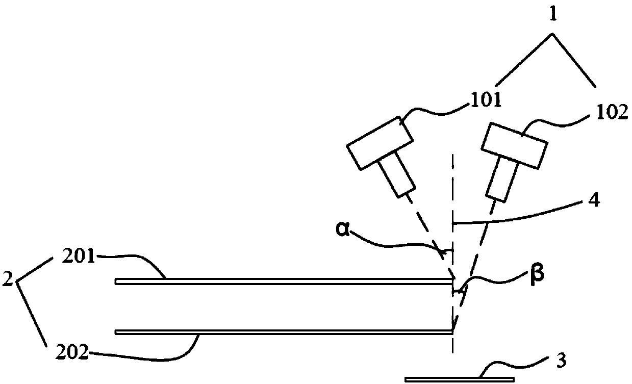
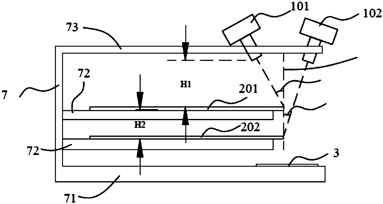
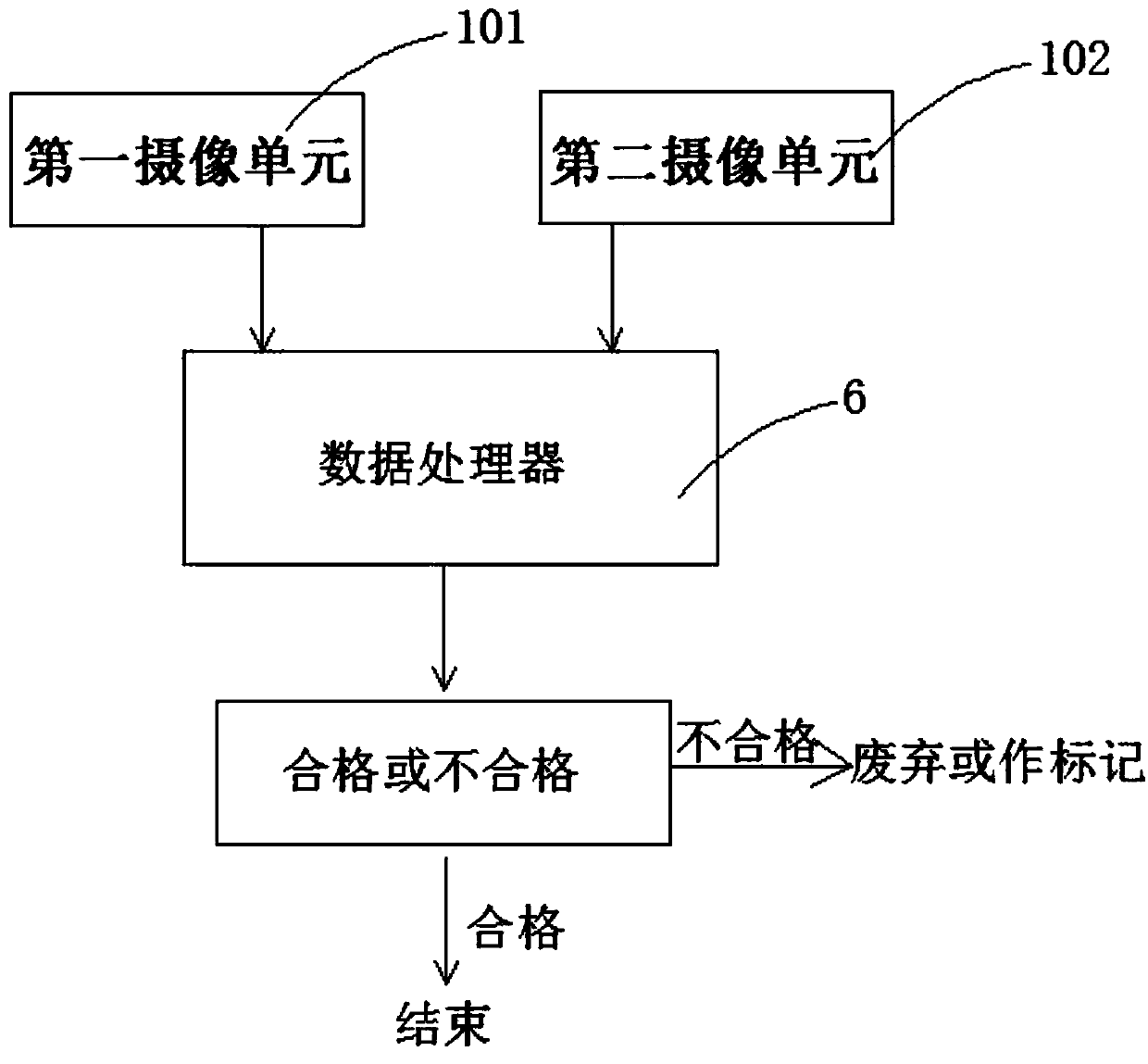
[0027] Such as figure 1 As shown, the embodiment of the present invention provides a device for detecting edge defects of a double-layer substrate, wherein the double-layer substrate 2 includes a first substrate 201 and a second substrate 202 arranged parallel thereto, and also includes a detection device 1 and an illumination unit 3 , the detection device 1 is arranged on one side of the double-layer substrate 2, the illumination unit 3 is arranged on the other side of the double-layer substrate 2, the detection device 1 includes a first camera unit 101 and a second camera unit 102, and the first camera unit 101 The first centerline of the first camera unit ...
PUM
 Abstract
Description
Claims
Application Information
 - Generate Ideas
- Intellectual Property
- Life Sciences
- Materials
- Tech Scout
- Unparalleled Data Quality
- Higher Quality Content
- 60% Fewer Hallucinations
Browse by: Latest US Patents, China's latest patents, Technical Efficacy Thesaurus, Application Domain, Technology Topic, Popular Technical Reports.
© 2025 PatSnap. All rights reserved.Legal|Privacy policy|Modern Slavery Act Transparency Statement|Sitemap|About US| Contact US: help@patsnap.com