Image sensor and preparation method thereof

An image sensor, a part of the technology, is used in electric solid state devices, semiconductor devices, radiation control devices and other directions, which can solve the problems of inability to meet market demand, high risk of multi-camera assembly, and high cost, and achieves reduction of manufacturing costs, reduction of chip area, The effect of simplifying the difficulty of assembly

Inactive Publication Date: 2018-05-01
HUAIAN IMAGING DEVICE MFGR CORP
View PDF4 Cites 2 Cited by
  • Summary
  • Abstract
  • Description
  • Claims
  • Application Information

AI Technical Summary

Problems solved by technology

[0005] However, the existing manufacturing process of front and rear dual cameras still has the problems of high cost and high risk of multi-camera assembly, which cannot meet market demand

Method used


Image

  • Image sensor and preparation method thereof
  • Image sensor and preparation method thereof
  • Image sensor and preparation method thereof

Examples


preparation example Construction

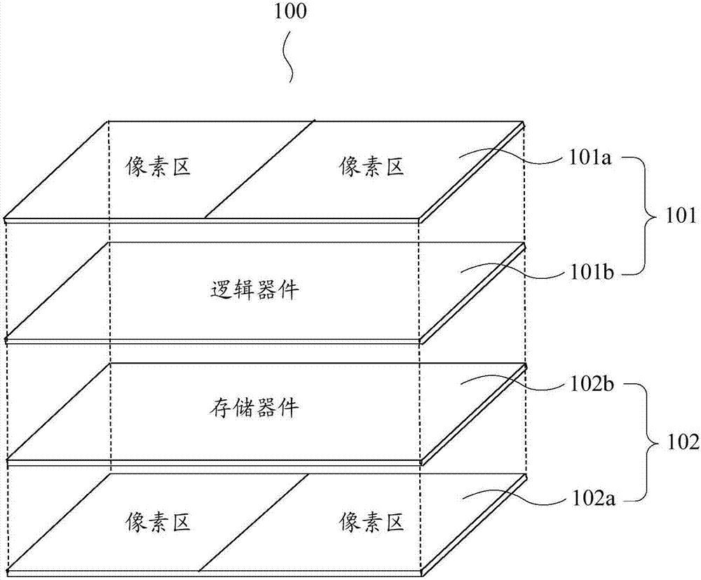
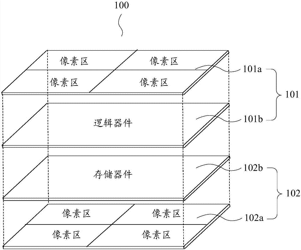
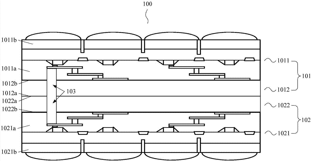
[0027] In order to solve the above technical problems, the technical solutions of the embodiments of the present invention provide an image sensor and a manufacturing method thereof, wherein the method includes: providing a first semiconductor substrate, and photosensitive pixels are formed on the front side of the first semiconductor substrate, and the The first semiconductor substrate is further formed with logic devices; a second semiconductor substrate is provided, and photosensitive pixels are formed on the front of the second semiconductor substrate; and the back of the first semiconductor substrate is bonded to the back of the second semiconductor substrate.

[0028] Those skilled in the art understand that the image sensor prepared by using the preparation scheme described in the embodiment of the present invention has a multi-layer structure, wherein the two outermost layers (ie, the front side of the first semiconductor substrate and the front side of the second semico...


PUM


Abstract

The invention discloses an image sensor and a preparation method thereof. The method comprises the following steps: providing a first semiconductor substrate, wherein photosensitive pixels are formedon the front face of the first semiconductor substrate, and a logic device is further formed on the first semiconductor substrate; providing a second semiconductor substrate, wherein photosensitive pixels are formed on the front face of the second semiconductor substrate; and bonding the back face of the first semiconductor substrate and the back face of the second semiconductor substrate. Throughthe scheme provided by the invention, the manufacturing cost of a front camera and a rear camera or multiple cameras can be effectively reduced, the assembling technology is simplified, and the areaof a chip is reduced.

Description

technical field [0001] The invention relates to the technical field of semiconductor manufacturing, in particular to an image sensor and a preparation method thereof. Background technique [0002] Image sensors are semiconductor devices that convert optical image signals into electrical signals. Among various image sensors, a Complementary Metal Oxide Semiconductor (CMOS) image sensor is widely used due to its advantages of small size, low power consumption, and low price. [0003] Existing CMOS image sensors mainly include front-side illumination (FSI for short) CMOS image sensors and back-side illumination (BSI for short) CMOS image sensors. Among them, the back-illuminated CMOS image sensor is more widely used because of its better photoelectric conversion effect, and the back-illuminated CMOS image sensor may also be called a back-illuminated CMOS image sensor. [0004] On the other hand, with the popularization of camera functions on portable electronic products such ...

Claims


Application Information

Patent Timeline
Patent Type & Authority Applications(China)
IPC IPC(8): H01L27/146
CPCH01L27/14634H01L27/1469
Inventor 佟璐陈世杰黄晓橹
Owner HUAIAN IMAGING DEVICE MFGR CORP
Why Eureka
Try Eureka