Method of manufacturing dielectric layer of grid

A technology of gate dielectric layer and manufacturing method, which is applied in the field of semiconductor element manufacturing, can solve the problems of reduced process yield, increased power consumption, and reduced component stability and reliability, so as to improve reliability and stability, prevent Effects of Junction Leakage and Avoidance of Thinning Phenomenon

A technology of gate dielectric layer and manufacturing method, which is applied in the field of semiconductor element manufacturing, can solve the problems of reduced process yield, increased power consumption, and reduced component stability and reliability, so as to improve reliability and stability, prevent Effects of Junction Leakage and Avoidance of Thinning Phenomenon

CN1917173AInactive Publication Date: 2007-02-21POWERCHIP SEMICON CORP

Image

  • Method of manufacturing dielectric layer of grid
  • Method of manufacturing dielectric layer of grid
  • Method of manufacturing dielectric layer of grid

Examples


Embodiment Construction

[0046] Figure 2A to Figure 2F To illustrate a cross-sectional view of a manufacturing process of a gate dielectric layer according to a preferred embodiment of the present invention.

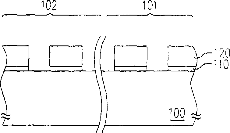
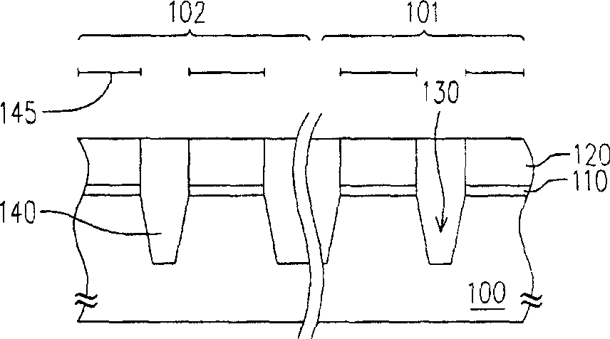
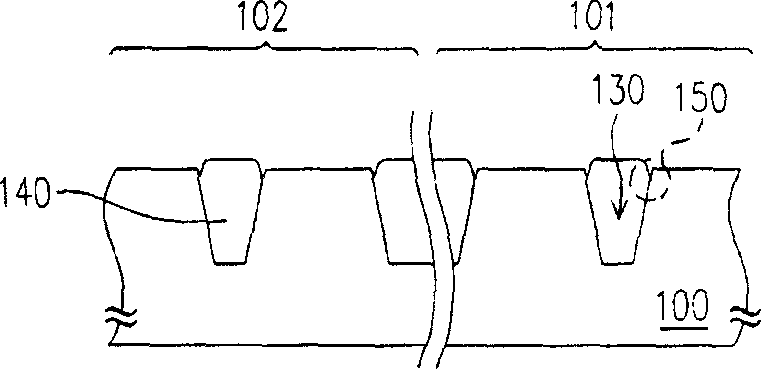
[0047] Please refer to Figure 2A In this manufacturing method, for example, the substrate 200 is provided first, and the substrate 200 can be at least divided into a high-voltage circuit area 201 and a low-voltage circuit area 202. Then take, for example, RCA solution (ammonia NH 4 OH and hydrogen peroxide H 2 O 2 The mixed solution of) performs a cleaning step on the substrate 200. After that, a dielectric layer 210 is formed on the substrate 200. The dielectric layer 210 is used as the gate dielectric layer in the high-voltage circuit area 201, so the thickness of the dielectric layer 210 is thicker than the conventional pad oxide layer, and the thickness of the dielectric layer 210 is about 200-1000 angstroms. The method of forming the dielectric layer 210 is, for example, a thermal oxidation m...


PUM

PropertyMeasurementUnit
Thicknessaaaaaaaaaa
Thicknessaaaaaaaaaa

Abstract

The method includes steps: first, the provided substrate can at least be divided into region of high voltage circuit and region of low voltage circuit; next, forming first dielectric layer on substrate, and the first dielectric layer is in use for grid dielectric layer in region of high voltage circuit; then, forming mask layer on the first dielectric layer, patterning the mask layer, the first dielectric layer, and the substrate in order to form groove in the substrate; forming insulating layer on the substrate to fill in the groove; removing the mask layer, and partial insulating layer to expose surface of the first dielectric layer; removing the first dielectric layer in region of low voltage circuit to expose surface of the substrate; forming second dielectric layer in substrate of the region of low voltage circuit' the thickness of the second dielectric layer is smaller than the first dielectric layer.

Description

Technical field [0001] The present invention relates to a method for manufacturing a semiconductor element, in particular to a method for manufacturing a gate dielectric layer. Background technique [0002] With the rapid development of the field of integrated circuits, high-efficiency, high-integration, low-cost, thin and short have become the goals pursued in the design and manufacture of electronic products. For the current semiconductor industry, in order to meet the above goals, it is often necessary to manufacture multiple functional components on the same chip. [0003] Integrating high-voltage components and low-voltage components on the same chip is a way to meet the above requirements. For example, low-voltage components are used to manufacture control circuits, and high-voltage components are used to manufacture Electrically Programmable Read-Only Memory (EPROM), Flash Memory, or liquid crystal display drive circuits. [0004] However, in order to be able to withstand ...

Claims


Application Information

Patent Timeline
21 Feb 2007
Publication
CN1917173A
IPC
H01L21/82
Inventors
้™ˆๆ–‡ๅ‰; ้™ˆไธœๆณข