A high dynamic cmos pixel unit

A pixel unit, high dynamic technology, applied in the field of image sensors, can solve problems such as difficulty in implementation, unsuitable for video applications, complex algorithms, etc., to achieve the effect of improving the dynamic range, increasing the effective photosensitive range, and increasing the saturated output voltage

Active Publication Date: 2020-06-30
SHANGHAI INTEGRATED CIRCUIT RES & DEV CENT +2
View PDF4 Cites 0 Cited by
  • Summary
  • Abstract
  • Description
  • Claims
  • Application Information

AI Technical Summary

Problems solved by technology

[0006] However, the above methods have certain limitations
For example, when using the above method 1), on the one hand, its algorithm is complicated, and on the other hand, it is not suitable for video applications because it requires multiple exposures
When the above method 2) is adopted, although this architecture can obtain an image whose output voltage has a logarithmic characteristic with the light intensity, this architecture also makes it difficult to guarantee the pixel consistency, making it difficult to realize

Method used


Image

  • A high dynamic cmos pixel unit
  • A high dynamic cmos pixel unit

Examples


Embodiment Construction

[0031] The specific embodiment of the present invention will be further described in detail below in conjunction with the accompanying drawings.

[0032] It should be noted that, in the following specific embodiments, when describing the embodiments of the present invention in detail, in order to clearly show the structure of the present invention for the convenience of description, the structures in the drawings are not drawn according to the general scale, and are drawn Partial magnification, deformation and simplification are included, therefore, it should be avoided to be interpreted as a limitation of the present invention.

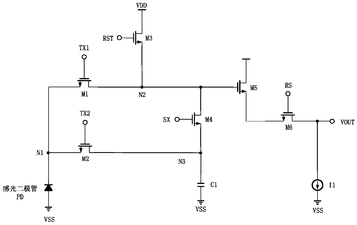
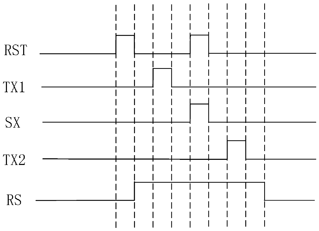
[0033] In the following specific embodiments of the present invention, please refer to figure 1 , figure 1 It is a schematic structural diagram of a high dynamic CMOS pixel unit circuit in a preferred embodiment of the present invention. Such as figure 1 As shown, a high dynamic CMOS pixel unit of the present invention may include: photodiode PD, ...


PUM


Abstract

The present invention disclosed a high -dynamic CMOS pixel unit, including: the light sensing diode, the first MOS tube, the fifth MOS tube, and the sixth MOS tube in turn;Between the first MOS tube and the fifth MOS tube, another polar connection capacitor of the fourth MOS tube; the second MOS tube, one pole is connected between the light sensing diode and the first MOS tube, and the other is connected to the first pole to the first poleBetween the four MOS tubes and the capacitor; the current source is connected to the output of the sixth MOS tube.The present invention can output low -light signals and high -light signals at the same time, and can process signal splicing by signal signals and high -light signals to increase the saturated output voltage of the pixel unit, which can increase the effective light range of pixel units, and and and of.As a result, the dynamic range of image sensors.The present invention also disclosed a signal collection and processing method of a high -dynamic CMOS pixel unit.

Description

technical field [0001] The present invention relates to the technical field of image sensors, in particular to a pixel unit of a high dynamic CMOS image sensor and a signal acquisition and processing method thereof. Background technique [0002] After decades of rapid development, CMOS image sensor technology has become more mature. With its advantages of low power consumption, low cost and high performance, CMOS image sensors have been widely used in various aspects. At the same time, with the advancement of technology and the diversity of application requirements, higher requirements are placed on CMOS image sensors. [0003] The HDR image sensor can perceive scenes under extremely low illumination and high illumination at the same time and in the same image. Such image sensors are widely used in national defense, industry, and life. Generally speaking, there are two ways to achieve high dynamic images: [0004] 1) For traditional image sensors, by changing the exposur...

Claims


Application Information

Patent Timeline
Patent Type & Authority Patents(China)
IPC IPC(8): H04N5/374H04N5/355
CPCH04N25/57H04N25/76
Inventor 段杰斌严慧婕温建新李琛罗颖
Owner SHANGHAI INTEGRATED CIRCUIT RES & DEV CENT
Why Eureka
Try Eureka