High dynamic cmos pixel unit and its signal acquisition method

A pixel unit and source technology, applied in the field of image sensors, can solve the problems of lower frame rate, low dynamic range of images, complex digital algorithms, etc., and achieve the effect of improving dynamic range and increasing effective photosensitive range

Active Publication Date: 2019-08-20
SHANGHAI INTEGRATED CIRCUIT RES & DEV CENT +1
View PDF8 Cites 0 Cited by
  • Summary
  • Abstract
  • Description
  • Claims
  • Application Information

AI Technical Summary

Problems solved by technology

The dynamic range of the traditional 4TCMOS pixel unit is not high in one exposure output image. High dynamic images can be achieved by combining images with multiple exposures, but it involves complex digital algorithms and will reduce the frame rate
Another method is to logarithmically output CMOS pixel units, but it has the problems of large process deviation of each pixel unit and poor pixel output consistency, making it difficult to achieve high-resolution applications

Method used


Image

  • High dynamic cmos pixel unit and its signal acquisition method
  • High dynamic cmos pixel unit and its signal acquisition method
  • High dynamic cmos pixel unit and its signal acquisition method

Examples


Embodiment Construction

[0025] In order to make the content of the present invention clearer and easier to understand, the content of the present invention will be further described below with reference to the accompanying drawings. Of course, the present invention is not limited to this specific embodiment, and general substitutions known to those skilled in the art are also covered within the protection scope of the present invention.

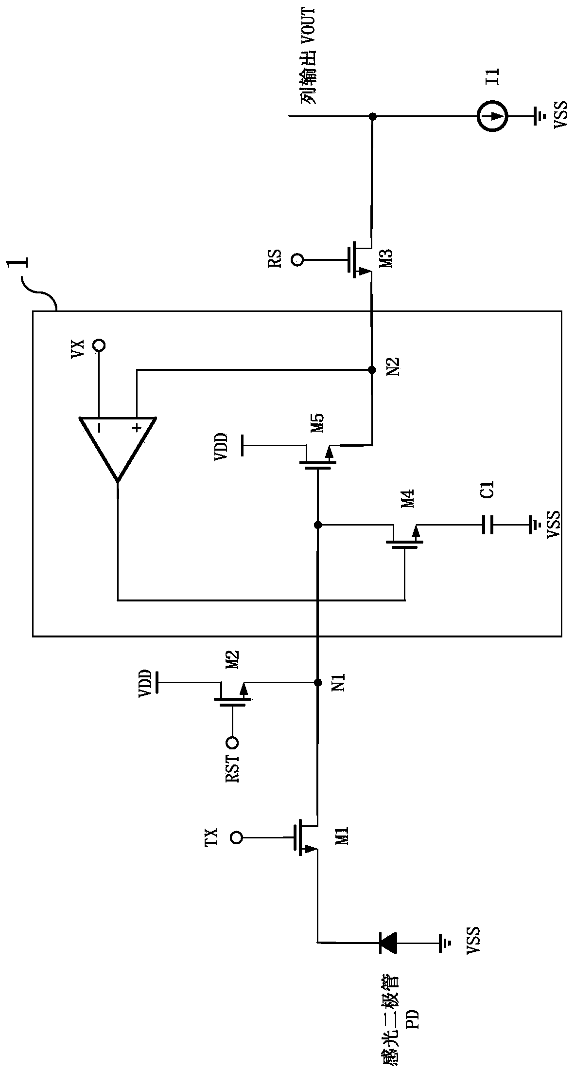
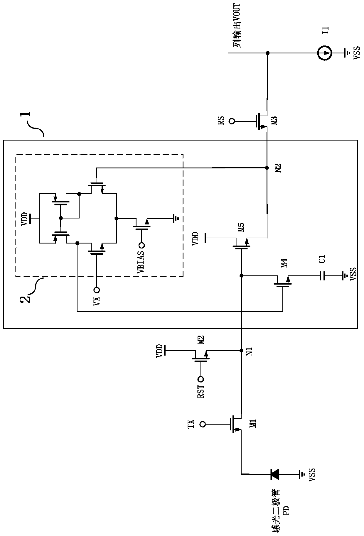
[0026] A CMOS pixel unit in the present invention includes: a power supply, a photosensitive diode, a strong light processing circuit, a column current source, a first NMOS transistor, a second NMOS transistor, a third NMOS transistor, and a column output terminal; wherein, the anode of the photosensitive diode It is connected to the negative pole of the power supply and is used to convert the optical signal into an electrical signal; the strong light processing circuit is connected to the drain of the first NMOS tube and the source of the second NMOS tube, and is us...


PUM


Abstract

The invention provides a CMOS pixel unit and a signal acquisition method thereof, comprising: the anode of the photosensitive diode is connected to the cathode of the power supply; the strong light processing circuit is connected to the drain of the first NMOS transistor and the source of the second NMOS transistor, It is used to add a storage capacitor for the electrical signal when the photosensitive diode is irradiated by strong light; the anode of the column current source is connected to the drain of the third NMOS gate, and is used as the signal output terminal of the high dynamic CMOS pixel unit, and the cathode of the column current source Connected to the negative pole of the power supply; the source of the first NMOS tube is connected to the cathode of the photosensitive diode for conducting the photosensitive diode; the source of the second NMOS tube is connected to the drain of the first NMOS tube, and the drain of the second NMOS tube The pole is connected to the positive pole of the power supply for resetting the output signal; the source of the third NMOS transistor is connected to the strong light processing circuit for selectively connecting each pixel unit to the column output.

Description

technical field [0001] The invention relates to the technical field of image sensors, in particular to a high dynamic CMOS pixel unit and a signal acquisition method thereof. Background technique [0002] CMOS image sensor has experienced rapid development in recent decades, and the technology has become more and more mature. With its advantages of low power consumption, low cost and high performance, it has been widely used in many fields of consumer electronics, monitoring, military, and aerospace. At the same time, with the development of the times, higher requirements are also put forward for CMOS image sensors. [0003] The dynamic range of human vision is as high as 200dB. The higher the dynamic range of CMOS image sensors, the more information the image provides, and the closer the image is to human vision. Therefore, high dynamic range CMOS image sensors are needed in the industry. The dynamic range of the output image of the traditional 4T CMOS pixel unit in one e...

Claims


Application Information

Patent Timeline
Patent Type & Authority Patents(China)
IPC IPC(8): H04N5/374H04N5/3745H04N5/355
CPCH04N25/59H04N25/77H04N25/76
Inventor 段杰斌温建新任铮皮常明张小亮
Owner SHANGHAI INTEGRATED CIRCUIT RES & DEV CENT
Why Eureka
Try Eureka