
Semiconductor device and manufacturing method therefor

A manufacturing method and semiconductor technology, applied in the direction of semiconductor/solid-state device manufacturing, semiconductor devices, electrical components, etc., can solve the problems of not fully considering SCSOA, etc., and achieve the effect of improving RBSOA and preventing the reduction of reverse withstand voltage

Inactive Publication Date: 2018-05-25
MITSUBISHI ELECTRIC CORP
View PDF6 Cites 1 Cited by
  • Summary
  • Abstract
  • Description
  • Claims
  • Application Information

AI Technical Summary

Problems solved by technology

Although it is necessary to design the impurity concentration of the deep low-concentration buffer layer within an appropriate range, the above-mentioned Japanese Patent Application Laid-Open No. 2011-119542 only discloses a certain degree of high concentration, and does not fully consider SCSOA.

Method used


Image

  • Semiconductor device and manufacturing method therefor
  • Semiconductor device and manufacturing method therefor
  • Semiconductor device and manufacturing method therefor

Examples


Embodiment approach 1

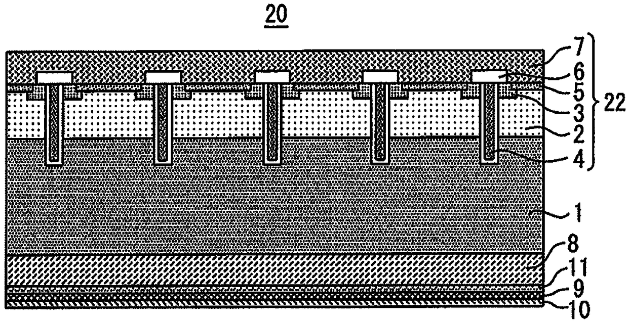
[0062] figure 1 It is a figure which shows the semiconductor device 20 which concerns on Embodiment 1 of this invention. The semiconductor device 20 according to Embodiment 1 is an insulated gate bipolar transistor (IGBT) including a trench gate. exist figure 1 Among them, a semiconductor device 20 includes a substrate 1 . Substrate 1 is made of silicon and has n-type conductivity. Since the substrate 1 functions as the drift layer 1 of the IGBT, the substrate 1 is also referred to as the drift layer 1 below.

[0063] On the drift layer 1, the MOSFET part 22 is provided by surface process. MOSFET portion 22 includes p-type base layer 2 , n + -type emitter layer 3 , trench gate 4 , p + -type layer 5 , interlayer insulating film 6 , and emitter electrode 7 . The p-type base layer 2 is disposed on the surface of the drift layer 1 . The p-type base layer 2 is pn-junctioned with the drift layer 1 to form a depletion layer. A plurality of n + -type emitter layers 3 are formed...

Embodiment approach 2

[0117] Figure 25 It is a figure which shows the semiconductor device 50 which concerns on Embodiment 2 of this invention. In Embodiment 1, the collector layer 9 is formed over the entire back side of the drift layer 1 . On the other hand, in Embodiment 2, the p-type collector layer 9 is formed directly under the cell portion 62 , and the p-type collector layer 9 is formed directly under the gate wiring portion 64 and the withstand voltage holding portion 66 . A p-type collector layer 14 having a low impurity concentration. Except for this point, the semiconductor device 50 according to the second embodiment has the same structure as the semiconductor device 20 according to the first embodiment. Therefore, the following description will focus on the differences from Embodiment 1, and the same or corresponding elements between Embodiment 1 and Embodiment 2 will be assigned the same reference numerals, and the description will be simplified or omitted.

[0118] Such as Figu...


PUM

PropertyMeasurementUnit
Resistivityaaaaaaaaaa
Thicknessaaaaaaaaaa
Thicknessaaaaaaaaaa

Abstract

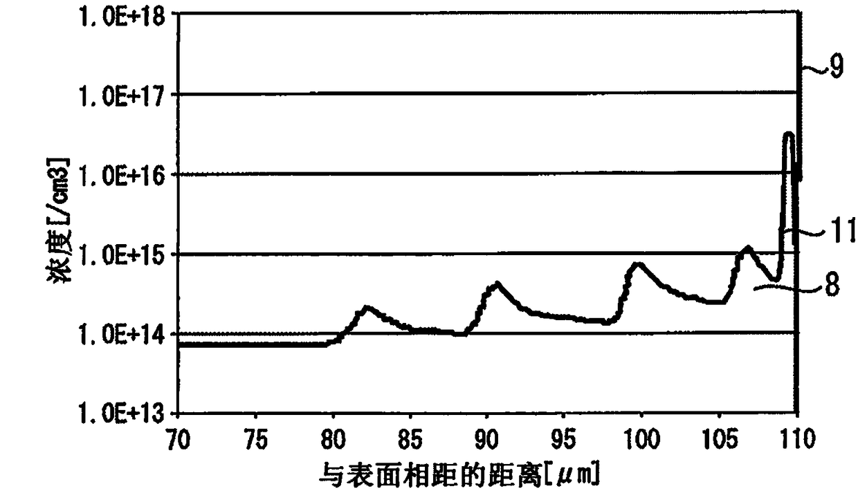
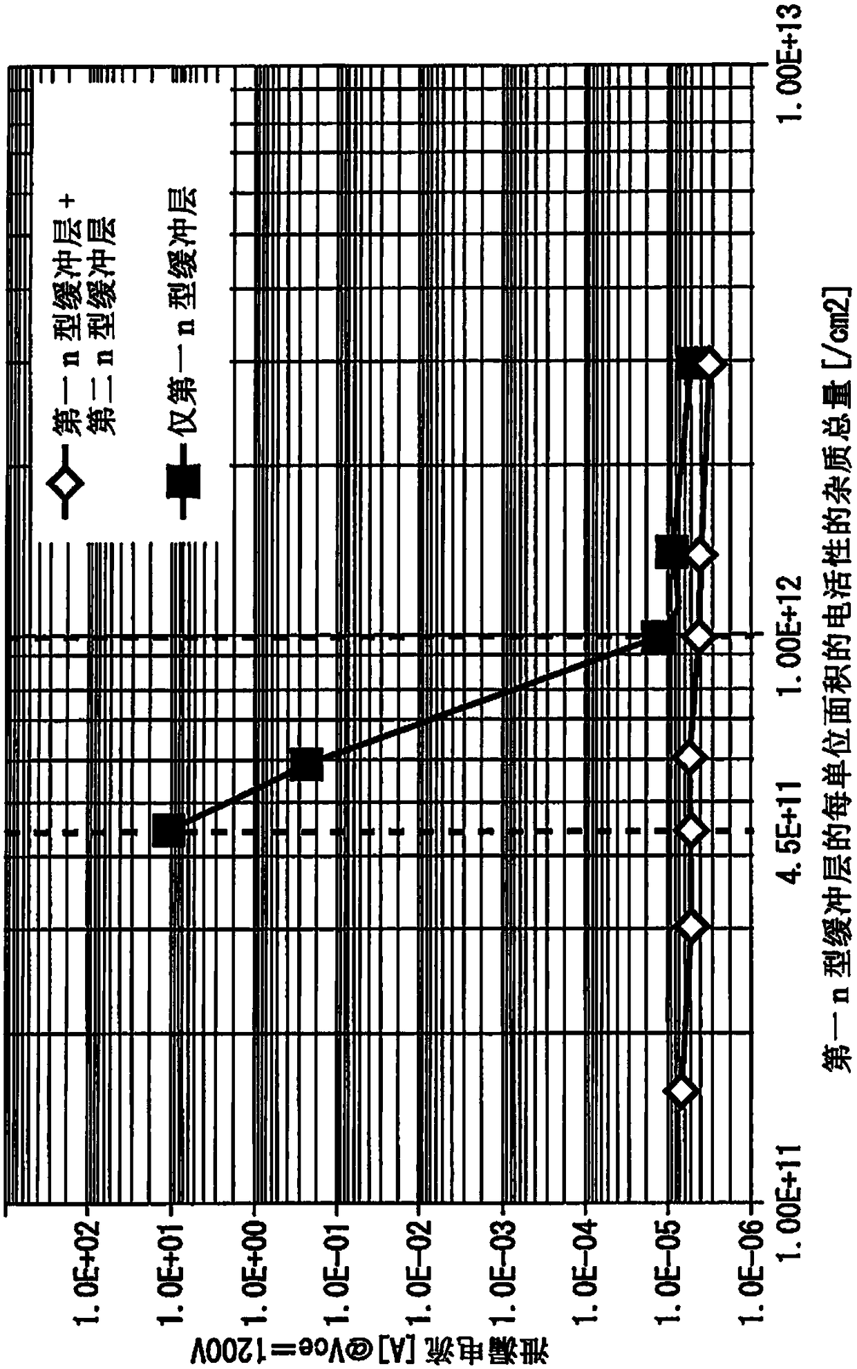
The present invention provides a semiconductor device with improved SCSOA while suppressing the leakage current and a manufacturing method therefor. A semiconductor device (20) includes a drift layer(1) formed of a first conductive type semiconductor material, a MOSFET part (22) including a p-type base layer (2) provided on a front surface of the drift layer (1), a first n-type buffer layer (8) provided on a reverse side of the drift layer (1), and a second n-type buffer layer (11) provided on a reverse side of the first n-type buffer layer (8) and having a high impurity concentration. The first n-type buffer layer (8) has a higher impurity concentration than the drift layer (1) and has a total amount of electrically active impurities per unit area of 1.0*10<12> cm<-2> or less.

Description

technical field [0001] The present invention relates to a semiconductor device. Background technique [0002] Conventionally, for example, as disclosed in JP 2011-119542 A, there is known an IGBT in which two buffer layers having different impurity concentrations are provided on the back side of the drift layer. The IGBT according to this publication includes: a low impurity concentration buffer layer on a side away from the p+ collector layer of the IGBT; and a high impurity concentration buffer layer on a side close to the p+ collector layer. [0003] One of the characteristics of the technique described in this publication is that the total thickness and total impurity amount of the low impurity concentration buffer layer and the high impurity concentration buffer layer fall within a certain range. In paragraph 0022 of this publication, regarding the specific structure of the buffer layer 24 as a low impurity concentration buffer layer, it is described that the impurity ...

Claims


Application Information

Patent Timeline
IPC IPC(8): H01L29/739H01L21/331
CPCH01L29/66348H01L29/7397H01L21/26506H01L21/26513H01L21/26586H01L29/36H01L29/32H01L29/0619H01L29/0638H01L29/4238H01L29/0834H01L21/047H01L29/0623H01L29/0696H01L29/1095H01L29/66068
Inventor 铃木健司高桥彻雄金田充上马场龙西康一
Owner MITSUBISHI ELECTRIC CORP
Learn More