Chip stripping device

A technology for stripping devices and chips, which is applied in the manufacture of electrical components, electrical solid devices, semiconductor/solid devices, etc., and can solve problems such as damage, chip failure, scratches, etc.

Inactive Publication Date: 2018-06-08
CETC BEIJING ELECTRONICS EQUIP
View PDF4 Cites 7 Cited by
  • Summary
  • Abstract
  • Description
  • Claims
  • Application Information

AI Technical Summary

Problems solved by technology

[0004] The purpose of the embodiments of the present invention is to provide a chip peeling device, which solves the problem that in the process of picking up and peeling u

Method used


Image

  • Chip stripping device
  • Chip stripping device
  • Chip stripping device

Examples


Embodiment Construction

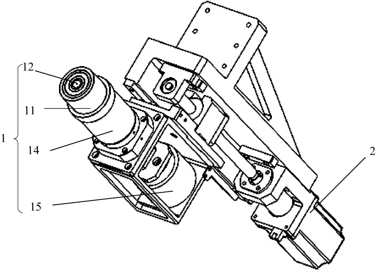
[0052] In order to make the technical problems, technical solutions and advantages to be solved by the present invention clearer, the following will describe in detail with reference to the drawings and specific embodiments.

[0053] Such as Figure 1 to Figure 3 As shown, the embodiment of the present invention provides a chip peeling device for peeling the blue film on the chip; including:

[0054] A device body 1, said device body 1 comprising:

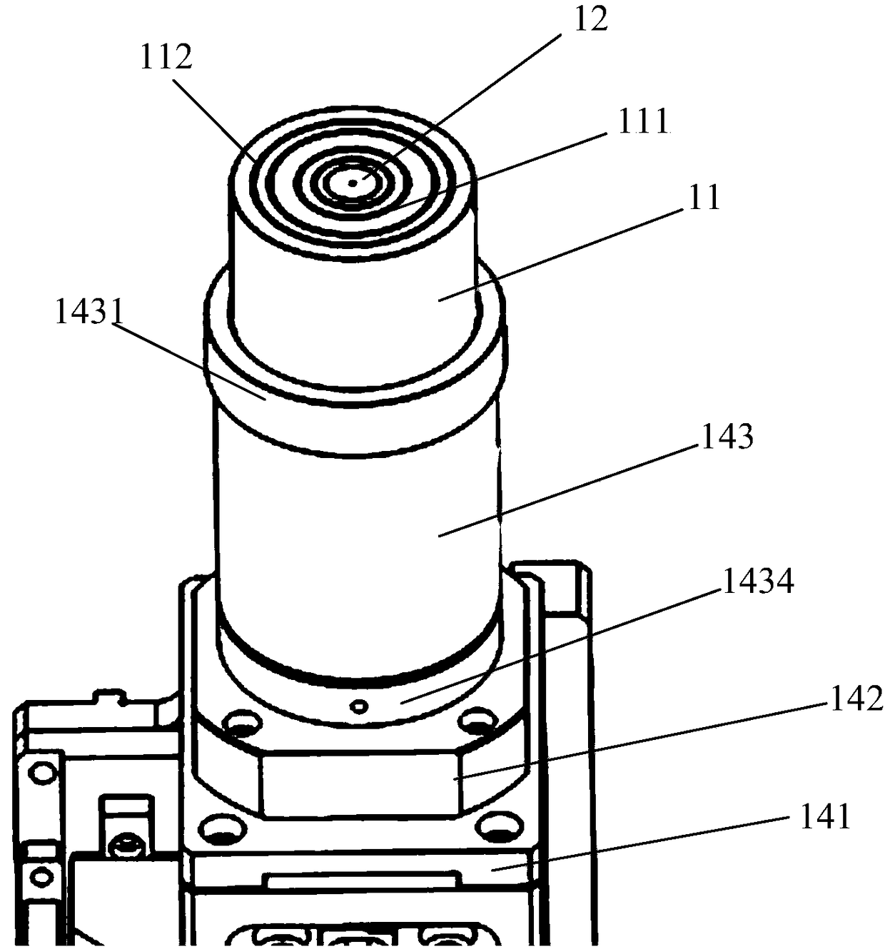
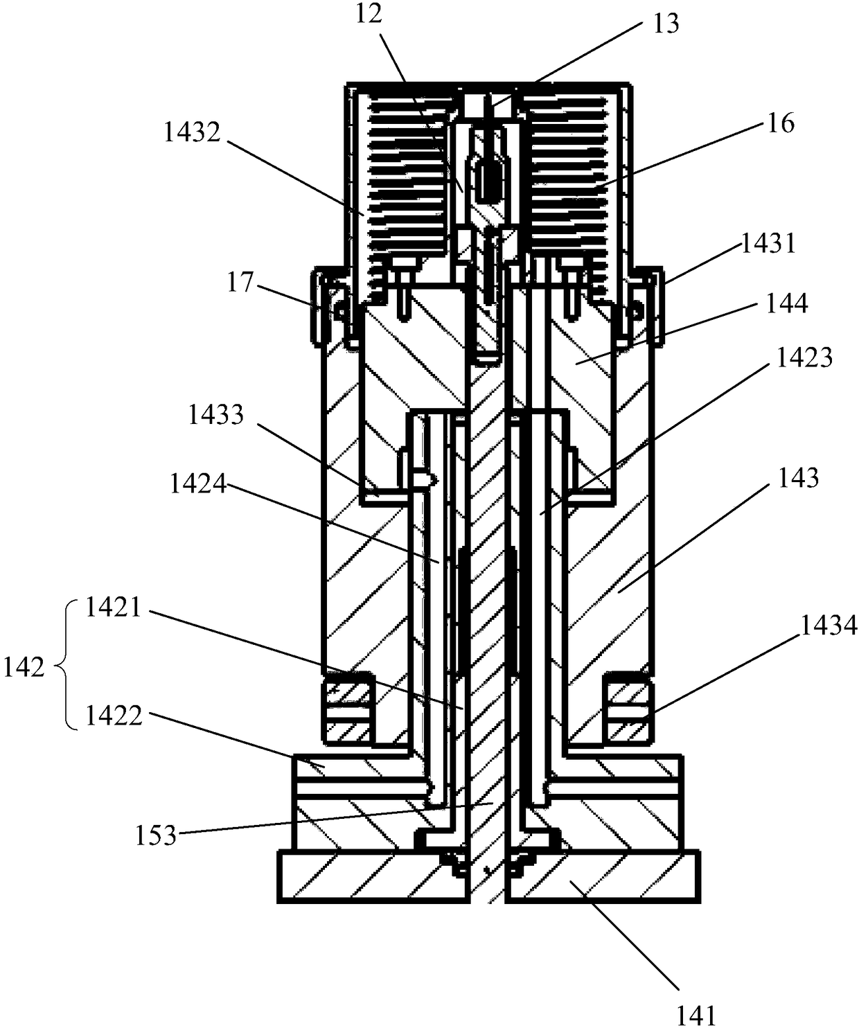
[0055] An adsorption platform 11 for adsorbing the blue film, the adsorption surface 111 of the adsorption platform is provided with a plurality of adsorption holes 112;

[0056] The boss 12 for pre-demolding the chip, the boss is arranged in the adsorption platform 11, and the adsorption platform 11 can move up and down in the direction perpendicular to the adsorption surface 111, so as to Make the boss 12 protrude from the adsorption surface 111 or be accommodated in the adsorption platform 11;

[0057] The thimble 13 for lift...


PUM


Abstract

The invention provides a chip stripping device. The chip stripping device includes an absorption platform used for absorbing a blue film, wherein an absorption face of the absorption platform is provided with a plurality of absorption holes; a boss used for pre-demolding a chip and arranged in the absorption platform capable of moving upward and downward in a direction perpendicular to the absorption face so as to enable the boss to protrude from the absorption face or to be accommodated in the absorption platform; a jacking needle used for jacking the chip so as to stripping the blue film andarranged in the boss and capable of moving upward and downward in a direction perpendicular to the absorption face relative to the boss so as to enable the jacking needle to protrude from the boss orto be accommodated in the boss; a first lifting mechanism used for driving the absorption platform to move upward and downward and connected with the absorption platform; and a second lifting mechanism used for driving the jacking needle to move upward and downward and connected with the jacking needle. In this way, the chip can be stripped gradually and chip failure can be avoided effectively.

Description

technical field [0001] The invention relates to the technical field of semiconductor packaging, in particular to a chip stripping device. Background technique [0002] With the development of the integrated circuit industry, integrated circuit (Integrated Circuit, referred to as IC) chips are becoming thinner and thinner, so IC packaging technology is developing rapidly in the direction of low power consumption, small size, high speed, and high integration. To meet the development needs of higher chip frequency, increased number of pins, reduced pin spacing, and improved reliability. As an indispensable key process step in the packaging process, the chip lift-off process plays an important role in the subsequent packaging process and product performance. At present, for the pick-up and peeling of ultra-thin chips below 50-100 μm, it is usually necessary to use the jacking force of the ejector pin of the chip peeling device to peel the chip from the blue film. However, since...

Claims


Application Information

Patent Timeline
IPC IPC(8): H01L21/67
CPCH01L21/67092H01L2221/68386
Inventor 沈会强霍杰郎平叶乐志崔洁
Owner CETC BEIJING ELECTRONICS EQUIP
Why Eureka
Try Eureka