Device and method for preparing polyimide dielectric layer and electronic circuit on curved surface

A polyimide medium and electronic circuit technology, which is applied in the manufacturing of printed circuits, electrical components, printed circuits, etc., can solve the problems of complexity, product shape limitation, and cumbersome manufacturing process, so as to simplify the manufacturing process and facilitate the Validate the effect of the work

Active Publication Date: 2019-05-31
西安瑞特三维科技有限公司
View PDF5 Cites 0 Cited by
  • Summary
  • Abstract
  • Description
  • Claims
  • Application Information

AI Technical Summary

Problems solved by technology

Through the processing technology of the above traditional electronic circuit, it can be seen that the manufacturing process is cumbersome, complicated and the cycle is long
At the same time, the microstrip antenna or thin film circuit printed on polyimide is limited by the shape of the product when it is finally shaped into the product. It cannot be formed on a non-expanded curved surface, and the shape of a regular curved surface also involves precision issues.
The current manufacturing process limits the application of dielectric layers and electronic circuits on curved surfaces and heterogeneous substrates, so a new process method is urgently needed to deal with the current processing and manufacturing problems

Method used


Image

  • Device and method for preparing polyimide dielectric layer and electronic circuit on curved surface
  • Device and method for preparing polyimide dielectric layer and electronic circuit on curved surface
  • Device and method for preparing polyimide dielectric layer and electronic circuit on curved surface

Examples


Embodiment Construction

[0035] Embodiments of the present invention are described in detail below, and the embodiments are exemplary and intended to explain the present invention, but should not be construed as limiting the present invention.

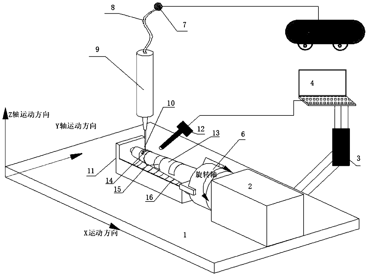
[0036] The basic principle of the present invention is to apply the printing method to coat the polyimide precursor solution PAA solution on the metal substrate, and form a PAA film, and then print the electronic circuit on the PAA film, or print the electronic circuit on the PAA film On the PI film generated by dehydration, the auxiliary heating device in the process can be formed at one time.

[0037] Such as figure 1 As shown, the device for preparing polyimide dielectric layer and electronic circuit on the curved surface in this embodiment includes a motion platform, a top seat, a heating device, a motor, a spray printing device, a temperature measuring device and a central controller.

[0038] The top base and the motor are installed on the motion platform...


PUM


Abstract

The invention provides a device and a method for preparing a polyimide dielectric layer and an electronic circuit on a curved surface. Based on a moving platform, by the aid of a 3D (three-dimensional) printing technology, prepared polyimide precursor solution with a certain concentration is printed on a curved surface substrate, electronic paste is printed on a formed film to form the electroniccircuit, the metal substrate is heated by an auxiliary heating device in the printing process, solvents in the polyimide precursor solution are promoted to rapidly volatilize, and film thickness unevenness caused by flow due to gravity action in the printing process is prevented. The device and the method can solve the problems of poor shaping precision, complicated forming process and the like due to the fact that shaping and gluing are performed after a circuit is printed on a traditional film. The polyimide dielectric layer and the electronic circuit can be prepared on the undeveloped curved surface once by the process technology, hand-made models related to the research and development process of the field of intelligent wear, conformal antennas, photovoltaic devices and the like are rapidly verified, and product research and development periods are shortened.

Description

technical field [0001] The invention relates to the technical field of preparing polyimide dielectric layers and electronic circuits on curved surfaces, in particular to a device and method for preparing polyimide dielectric layers and electronic circuits on curved surfaces. Background technique [0002] At present, with the development of the electronics industry, the demand for curved surface electronic circuits in industries such as photovoltaics, mobile phone antennas, and microwave antennas is becoming more and more obvious. Polyimide is one of the organic polymer materials with the best comprehensive performance, high temperature resistance up to 400 °C, high insulation performance, dielectric constant of 4.0 at 103 Hz, and dielectric loss of only 0.004 to 0.007, so it is often used as a microstrip antenna And the dielectric layer of flexible circuits. [0003] The manufacturing process of the traditional microstrip antenna is to combine the copper foil and polyimide ...

Claims


Application Information

Patent Timeline
Patent Type & Authority Patents(China)
IPC IPC(8): H05K3/12
CPCH05K3/125H05K2203/0126H05K2203/1131
Inventor 李超尹恩怀
Owner 西安瑞特三维科技有限公司
Why Eureka
Try Eureka