Chip awakening method and circuit

A wake-up circuit and chip technology, applied in electrical components, electronic switches, pulse technology, etc., can solve the problem that the chip wake-up circuit is not suitable for monitoring chips, etc., and achieve the effects of preventing false triggering, prolonging the service life, and avoiding false starts

Active Publication Date: 2018-06-15
DATANG NXP SEMICON CO LTD
View PDF6 Cites 9 Cited by
  • Summary
  • Abstract
  • Description
  • Claims
  • Application Information

AI Technical Summary

Problems solved by technology

[0004] The invention provides a chip wake-up method to solve the problem that the existing chip wake-up circuit is not suitable for low-frequency communication car battery monitoring chips

Method used


Image

  • Chip awakening method and circuit
  • Chip awakening method and circuit
  • Chip awakening method and circuit

Examples


Embodiment 1

[0039] A chip wake-up circuit provided by an embodiment of the present invention is introduced in detail.

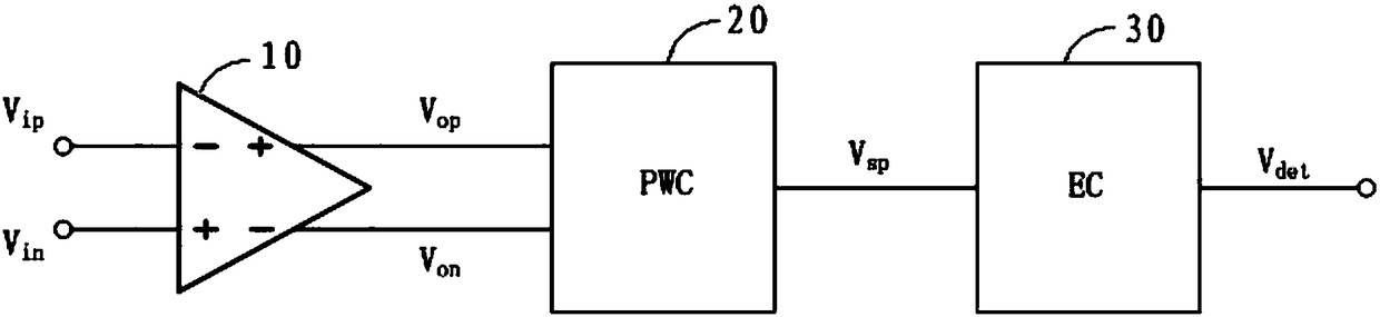
[0040] refer to figure 1 , shows a structural diagram of a chip wake-up circuit in an embodiment of the present invention, the circuit includes: a band-pass dynamic amplifier 10, a pulse width comparator 20, and an edge counter 30 connected in sequence;

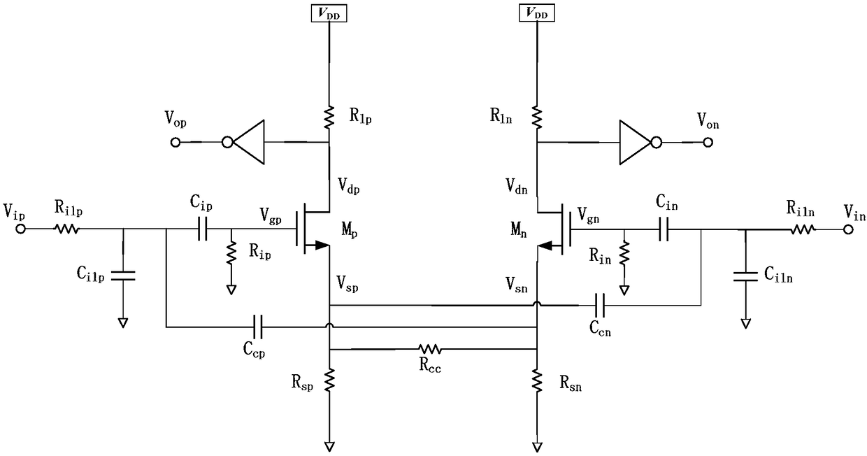
[0041] Described band-pass dynamic amplifier 10 comprises band-pass filter, amplifying tube M p , M n ; The bandpass filter is coupled to the amplifier tube M respectively p , M n The gate and source of the input to filter the high and low frequency signal interference, see figure 2 ;

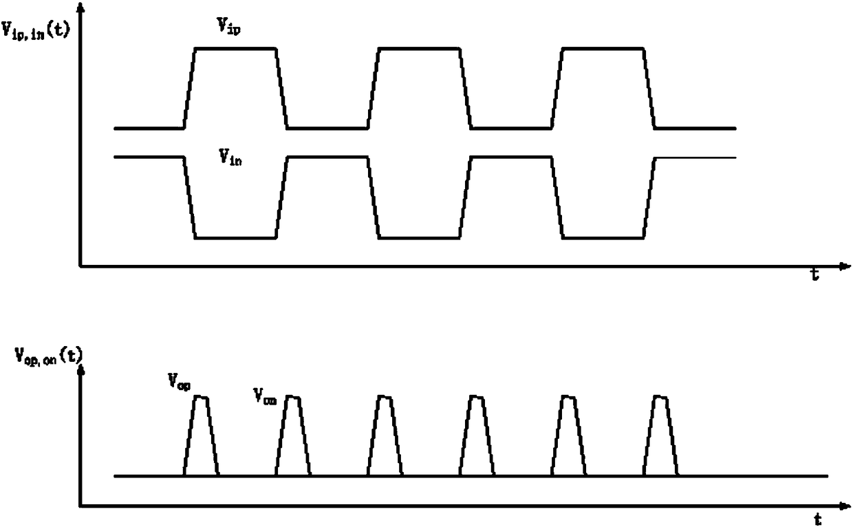
[0042] When the input signal of the band-pass dynamic amplifier is a differential low-frequency signal and the differential mode level meets the set level range, the rising edge and falling edge of the pulse signal output by the pulse width comparator meet the set time interval, and the When the number of pulses recorded by the ed...

Embodiment 2

[0066] refer to Image 6 , shows a flow chart of a method for waking up a chip in another embodiment of the present invention. The methods include:

[0067] Step 201, check whether the chip wake-up circuit meets the set conditions: the input signal of the band-pass dynamic amplifier is a differential low-frequency signal and the differential mode level meets the set level range; the rising edge and falling edge of the pulse signal output by the pulse width comparator The set time interval is met; the number of pulses recorded by the edge counter reaches the set threshold.

[0068] In this embodiment, the chip wake-up circuit is obtained through Embodiment 1. The input signal of the band-pass dynamic amplifier is a differential low-frequency signal, which meets the frequency of use of the car battery monitoring chip; the differential mode level meets the set level range, that is, the voltage of the differential low-frequency signal reaches the turn-on voltage of the amplifier...


PUM


Abstract

The invention provides a chip awakening method and circuit. The circuit comprises a bandpass dynamic amplifier, a pulse width comparator and an edge counter that are connected in sequence, wherein thebandpass dynamic amplifier comprises a bandpass filter and an amplification tube, and the bandpass filter is coupled to a gate and a source of the amplification tube separately. The method comprisesthe steps of detecting whether the chip awakening circuit meets preset conditions, wherein the preset conditions are as follows: an input signal of the bandpass dynamic amplifier is a differential lowfrequency signal and a differential mode level is within a preset level range; an ascending edge and a descending edge of a pulse signal output by the pulse width comparator meet a preset time interval; and the number of pulses recorded by the edge counter reaches a preset threshold; if all the preset conditions are met, outputting an awakening signal. Through adoption of the chip awakening method and circuit, the chip awakening circuit avoids false triggering, so that a battery monitor chip avoids false tripping, and the service life of the battery is prolonged.

Description

technical field [0001] The invention relates to the technical field of automobile battery chips, in particular to a chip wake-up method and circuit. Background technique [0002] The application of the wake-up circuit is mainly to save power consumption. Usually, signal communication requires a lot of power consumption. When there is no signal transmission, the signal transceiver circuit can be put in a dormant state until the wake-up circuit detects that there is a signal input. [0003] The wake-up circuit has a wide range of applications, and is often used in wireless network systems such as WSN (Wireless Sensor Network, Wireless Sensor Network), WPN (Wireless Personal Area Network, Wireless Personal Area Network), or USB (Universal Serial Bus, Universal Serial Bus), LAN (Local Area Network, Local Area Network), CAN (Controller Area Network, Controller Area Network) and other wired communication networks. With the wake-up circuit, the system can formulate an efficient en...

Claims


Application Information

Patent Timeline
Patent Type & Authority Applications(China)
IPC IPC(8): H03K17/30
Inventor 张文翩刘艳娇
Owner DATANG NXP SEMICON CO LTD
Why Eureka
Try Eureka