OLED substrate and preparation method and display device thereof
A substrate and substrate technology, used in semiconductor/solid-state device manufacturing, semiconductor devices, electrical components, etc., can solve the problems of luminescent layer material deposition, lowering the resolution of OLED substrates, color mixing, etc., to reduce the distance and achieve better display effects. , the effect of increasing the resolution
- Summary
- Abstract
- Description
- Claims
- Application Information
AI Technical Summary
Problems solved by technology
Method used
Image


Examples
Embodiment 1
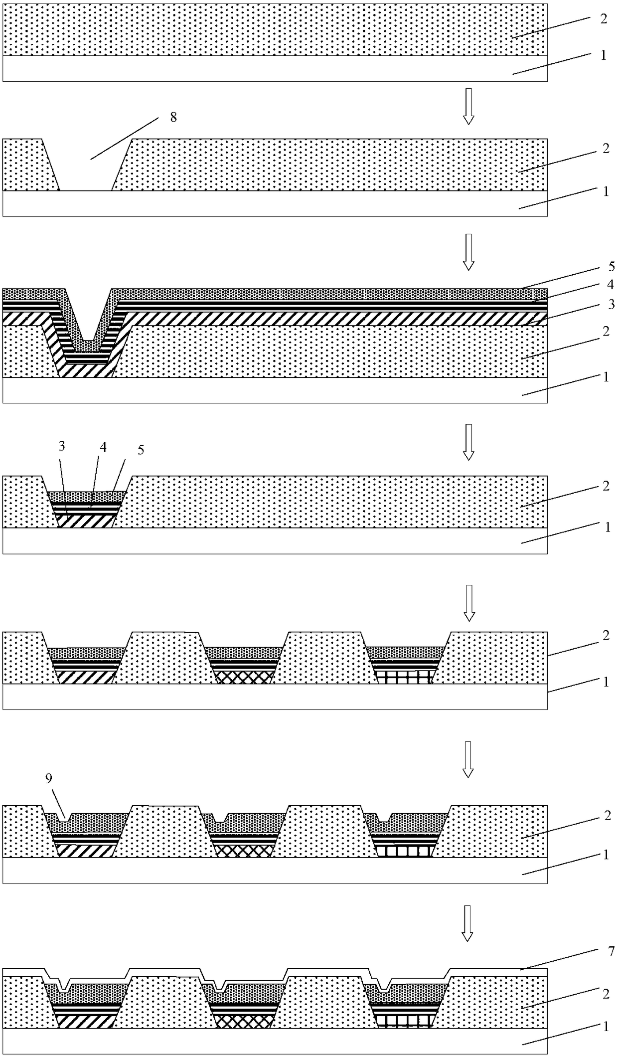
[0038] Such as figure 1 As shown, the present embodiment provides a method for preparing an OLED substrate, comprising the following steps: forming a pixel defining layer 2 on a substrate 1, and forming an accommodating portion 8 of an OLED device of one color in the pixel defining layer 2; In the container part 8 formed in the step, the light emitting layer 3, the cathode layer 4, and the encapsulation layer 5 arranged in sequence along the direction away from the substrate 1 are formed; according to the above steps, the container parts of OLED devices of other colors are formed in the pixel definition layer 2 one by one 8; and, after forming the containing portion 8 of the OLED device of one color, in the formed containing portion 8, the light emitting layer 3, the cathode layer 4, and the encapsulating layer 5 of the OLED device of the color are sequentially formed.
[0039] Further, the preparation method of the OLED substrate in this embodiment also includes: after formin...
Embodiment 2
[0042] Such as figure 2 As shown, the present embodiment provides a method for preparing an OLED substrate, which includes the following steps:
[0043] Step 1, forming a pixel driving circuit on the substrate 1 .
[0044] Specifically, on the substrate 1 , various layer structures including switching transistors, driving transistors, storage capacitors and other elements are formed through a patterning process to form a pixel driving circuit.
[0045] Step 2: On the substrate 1 after the above step 1, the anode layer of each OLED device is formed by a patterning process.
[0046] It should be noted that the anode layer of each OLED device is connected to the drain of the driving transistor of the corresponding pixel driving circuit. Usually, it is necessary to form an interlayer insulating layer on each layer structure of the formed pixel driving circuit, and etch the interlayer insulating layer to form a via hole 9 for connecting the drain of the driving transistor of the...
Embodiment 3
[0061] Such as image 3 As shown, this embodiment provides an OLED substrate, which can be prepared by the method for preparing the OLED substrate provided in Embodiment 1 or Embodiment 2. Wherein, the OLED substrate comprises: a substrate 1; a pixel defining layer 2, in which an accommodating portion 8 is arranged; along a direction away from the substrate 1, the light-emitting layer 3 and the cathode layer of the OLED device arranged sequentially in the accommodating portion 8 4. Encapsulation layer 5; wherein, the cathode layer 4 and the encapsulation layer 5 of each OLED device are independently arranged and disconnected from each other, so as to protect the light emitting layer 3, so as to prevent the formation of a certain color light emitting layer 3 , contaminate already formed luminescent layers 3 of other colors.
[0062] Among them, such as Figure 4 As shown, preferably in the present embodiment, the OLED substrate further includes: a protective layer 6, which is...
PUM
| Property | Measurement | Unit |
|---|---|---|
| Particle size | aaaaa | aaaaa |
Abstract
Description
Claims
Application Information