DGS filter, printed circuit board, and filtering device

A printed circuit board and filter device technology, applied in the field of communication, can solve the problems of unsuitable multilayer printed circuit boards and reduced filtering ability of DGS filters, etc.

Active Publication Date: 2018-07-03
HUAWEI TECH CO LTD +1
4 Cites 6 Cited by

AI-Extracted Technical Summary

Problems solved by technology

[0003] However, for a communication substrate formed by a multilayer printed circuit board (that is, a printed circuit board including multiple wiring layers and multiple ground substrates), if the above-mentioned defective ground structure is only provided on on...

Method used

After the common mode insertion loss that the multilayer printed circuit board 200 shown in Figure 10 produces is simulated, the simulation result obtained is as shown in Figure 11, as can be seen, compared to the above-mentioned DGS figure 22 that is not provided with Printed circuit board, the printed circuit board 200 provided by the embodiment of the present invention can suppress the common mode insertion loss below -10dB in the 6GHz bandwidth of about 25GHz-31GHz, thereby reducing the differential signal transmission on the differential line 21. Common mode noise to ensure the filtering capability of the DGS pattern 22 on the multilayer printed circuit board.
After the common mode insertion loss that the multilayer printed circuit board 400 shown in Figure 14 produces is simulated, the simulation result obtained is as shown in Figure 15, as can be seen, compared to the above-mentioned DGS figure 22 that is not provided with Printed circuit board, the printed circuit board 400 provided by the embodiment of the present invention can suppress the common mode insertion loss below -10dB in the 2GHz bandwidth of about 20GHz-22GHz, thereby reducing the diff...

Abstract

The embodiment of the invention, which relates to the field of the communication technology, provides a defected ground structure (DGS) filter, a printed circuit board, and a filtering device so thatthe filtering capability of a DGS filter on a multilayer printed circuit board can be strengthened. The DGS filter being configured to filter a signal transmitted on target routing in a first routinglayer in a printed circuit board is composed of a first reference layer and a target layer that are arranged in opposite. The target layer is a reference layer different from the first reference layerin the printed circuit board or a routing layer different from the first routing layer in the printed circuit board. A DGS pattern is arranged in the first reference layer and is arranged in symmetric distribution by using the vertical projection of the target routing in the first reference layer as a symmetric axis. N ground via holes are formed and penetrate the first reference layer and the target layer; and the first reference layer is communicated with a reference area in the target layer through the N ground via holes.

Application Domain

Printed electric component incorporationWaveguide type devices

Technology Topic

Printed circuit boardSymmetric axis +1

Image

  • DGS filter, printed circuit board, and filtering device
  • DGS filter, printed circuit board, and filtering device
  • DGS filter, printed circuit board, and filtering device

Examples

  • Experimental program(1)

Example Embodiment

[0038] The technical solutions in the embodiments of the present invention will be described in detail below in conjunction with the drawings in the embodiments of the present invention.
[0039] In addition, the terms "first" and "second" are only used for descriptive purposes, and cannot be understood as indicating or implying relative importance or implicitly indicating the number of indicated technical features. Thus, the features defined with "first" and "second" may explicitly or implicitly include one or more of these features. In the description of the present invention, unless otherwise specified, "plurality" means two or more.
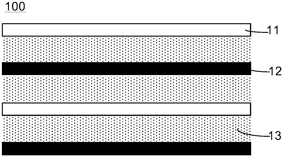
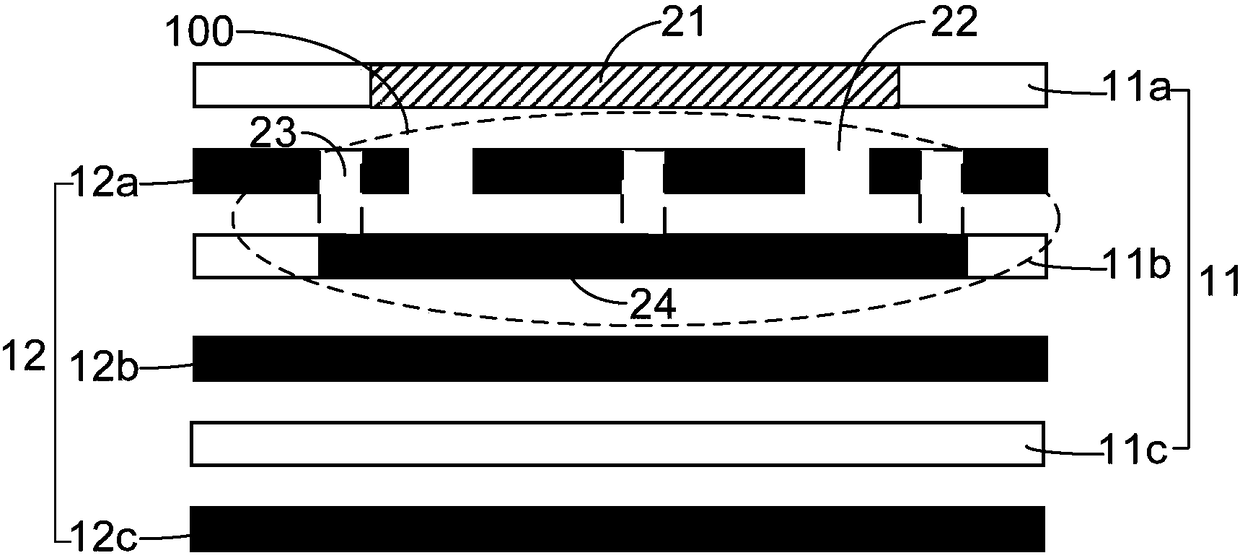
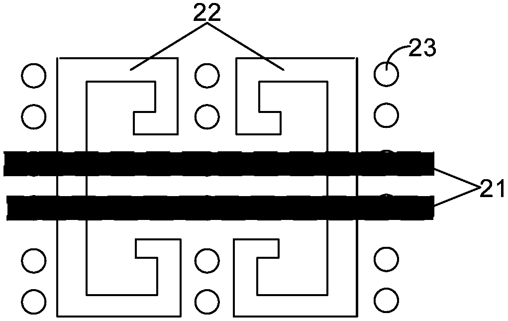
[0040] The DGS filter provided by the embodiment of the present invention can be applied to a multilayer printed circuit board, the multilayer printed circuit board includes at least two reference layers and at least two wiring layers, and each wiring layer corresponds to one The reference layer (or multiple wiring layers may correspond to the same reference layer), and the reference layer provides a reference ground signal for the wiring layer.
[0041] Exemplarily, when each routing layer uniquely corresponds to a reference layer, such as figure 1 As shown, the wiring layer 11 and the reference layer 12 in the multilayer printed circuit board 100 are alternately arranged in sequence. In other words, the multilayer printed circuit board 100 includes a plurality of wiring layers 11, and each wiring layer 11 is correspondingly provided with a reference layer 12. Moreover, any adjacent wiring layer 11 and the reference layer 12 can be filled with an insulating dielectric layer 13. In order to facilitate the description of the DGS filter provided by the embodiment of the present invention, the following embodiments will use figure 1 The wiring layer 11 and the reference layer 12 alternately arranged in sequence are shown as an example for description.
[0042] Wherein, the wiring layer 11 is generally provided with wiring for carrying electrical signals, which can be specifically composed of one or more metal wirings, and the reference layer 12 is generally used for carrying power or reference ground signals, and the metal wiring in the wiring layer 11 The electrical signal carried by the wire is finally led to each input/output (I/O, in/out) interface of the printed circuit board 100.
[0043] Such as figure 2 As shown, the DGS filter 100 provided by the embodiment of the present invention is used to filter the signal transmitted on the target trace in the first trace layer 11a. Wherein, the wire can be a differential wire 21 or a single wire, which is not limited in the embodiment of the present invention.
[0044] Take the above target trace as an example of the differential line 21, such as figure 2 As shown, the DGS filter 100 includes: a first reference layer 12a and a target layer 11b arranged oppositely. The target layer 11b can be any reference layer in the printed circuit board except the first reference layer 12a, or it can be a printed circuit board. Any wiring layer in the circuit board except the first wiring layer 11a ( figure 2 The wiring layer 11b is the above-mentioned target layer).
[0045] Specifically, a DGS pattern 22 is provided in the first reference layer 12a, such as image 3 As shown, the DGS pattern 22 is symmetrically distributed with the vertical projection of the differential line 21 in the first reference layer 12a as the symmetry axis. The shape of the DGS pattern 22 may be a double C-shaped defect structure or a U-shaped dumbbell-shaped defect structure in the prior art, or may be a structure with other defects, which will be described in detail in subsequent embodiments of the present invention.
[0046] Among them, combined figure 2 with image 3 As shown, on the periphery of the DGS pattern 22, along the direction perpendicular to the first reference layer 12a, N (N>1) ground vias 23 are provided through the first reference layer 12a and the target layer 11b, such as figure 2 As shown, the first reference layer 12a communicates with a reference ground area 24 provided in the target layer 11b through a ground via 23. Although each area in each reference layer 12 can provide a reference ground signal, in the embodiment of the present invention, the area where the DGS pattern 22 is projected in any reference layer can be used as the reference ground area, and in any wiring layer Inside, you can also set the area where the DGS graphics are projected as the reference area.
[0047] It should be noted that in figure 2 In the DGS filter 100 shown, the ground via 23 connects the first reference layer 12a and the reference ground area 24 in the wiring layer 11b (ie, the target layer) adjacent to the first reference layer 12a.
[0048] Understandably, such as Figure 4 As shown, the ground via 23 may also communicate with the reference ground area in the multilayer wiring layer 11 and the multilayer reference layer 12. For example, in Figure 4 In (a), the ground via 23 penetrates all the wiring layers 11 of the printed circuit board (that is, the wiring layer 11a, the wiring layer 11b, and the wiring layer 11c) 11 and all the reference layers 12 (that is, the reference layer 12a, reference layer 12b, and reference layer 12c); Figure 4 In (b), the ground via 23 penetrates the first reference layer 12a where the DGS pattern 22 is located, the target layer 11b, and the reference layer 12b between the first reference layer 12a and the target layer 11b.
[0049] In other words, the above-mentioned ground via 23 may be a through hole, a blind hole or a buried hole, which is not limited in the embodiment of the present invention.
[0050] To Figure 4 In (b) as an example, when the local via 23 is a buried hole, since the ground via 23 only penetrates the first reference layer 12a, the target layer 11b, and the reference layer 12b, then the ground via 23 is not provided. The wiring layer 11c can also be wired normally, thereby reducing the influence on the wiring in the multilayer printed circuit board.
[0051] It can be seen that for the multilayer printed circuit board, in the DGS filter provided by the embodiment of the present invention, N ground vias can be arranged on the periphery of the DGS pattern, and further, different references can be made through these N ground vias. The reference ground areas between layers or wiring layers are connected, so that the reference potentials of the reference ground areas between different reference layers or wiring layers are the same, thereby reducing the resonance between different reference layers or wiring layers to ensure multiple layers The filtering capability of the DGS filter on the printed circuit board.
[0052] Optionally, the distance between any two adjacent ground vias 23 is not greater than 1/4 of the maximum operating wavelength of the DGS filter 100. For example, the working frequency band of the DGS pattern 22 is 25GHz-30GHz, that is to say, the maximum working frequency of the DGS pattern 22 is 30GHz. When the DGS pattern 22 works at 30GHz, the wavelength of the electromagnetic wave radiated by it is λ (λ>0), Then, the distance p between any two adjacent ground vias 23 should be less than or equal to λ/4.
[0053] When the distance between two adjacent ground vias is not greater than 1/4 of the maximum working wavelength of the DGS filter, these N ground vias are equivalent to forming a hole grid in the multilayer printed circuit board. The N ground vias are arranged on the periphery of the DGS pattern. Therefore, the DGS pattern in the printed circuit board is equivalent to being wrapped by the hole grid formed by the N ground vias, which can shield the electromagnetic waves generated by the DGS filter. So as to effectively suppress the electromagnetic radiation generated by the DGS filter.
[0054] Optional, such as figure 2 As shown, in the first reference layer 12a, the above-mentioned N ground vias 23 can be set to surround the periphery of the DGS pattern 22 to form a closed pattern, that is, form as Figure 5 The N ground vias 23 are shown, so that the DGS pattern 22 can be more completely wrapped by the adjacent reference ground area 24 and the surrounding N ground vias 23, which can further suppress the electromagnetic radiation generated by the DGS filter .
[0055] Further, a hollowed-out layer may be provided between the first reference layer and the target layer. At this time, the hollowed-out layer 31 may be filled with an insulating medium, for example, such as Image 6 As shown in (a), the first reference layer is 12a, and the routing layer 11b can be hollowed out to form a hollowed-out layer 31a. The size of the vertical projection of the hollowed-out layer 31 on the first reference layer 12a is the same as The sizes of the patterns formed by the vias 23 on the first reference layer 12a are the same. At this time, the target layer is the reference layer 12b; or, as Image 6 As shown in (b), the first reference layer is 12a, and the routing layer 11b and reference layer 12b can be hollowed out to form a hollowed-out layer 31b. At this time, the target layer is the routing layer 11c. The vertical projection of layer 31 on the target layer 11c overlaps with the reference area 24 in the target layer 11c; or, as Image 6 As shown in (c), the first reference layer is 12a, and the routing layer 11b, reference layer 12b, and routing layer 11c can be hollowed out to form a hollowed-out layer 31c. At this time, the target layer is the reference layer 12c . When the depth of the hollowed-out layer is greater, the suppression effect on common mode noise is more obvious, and the working bandwidth of the DGS filter also increases.
[0056] It can be seen that no matter how many reference layers or wiring layers are hollowed out, the reference ground area in the target layer, the hollowed-out layer, and the N ground vias around the DGS graphics together form an inclusion to suppress the DGS filter. Electromagnetic radiation.
[0057] Optionally, the first wiring layer may be a wiring layer located on the surface of the DGS filter (such as figure 2 , Figure 4 or Image 6 The first wiring layer 11a) shown can also be a wiring layer located at the bottom layer in the above-mentioned multilayer printed circuit board, or any wiring layer located in the middle layer of the above-mentioned multilayer printed circuit board. The embodiment of the invention does not limit this.
[0058] It should be noted, figure 2 , Figure 4 as well as Image 6 The DGS filter 100 shown in can be used as part of a printed circuit board, figure 2 , Figure 4 as well as Image 6 The reference layer 12 of the DGS filter 100 shown in is not necessarily used as the reference layer of the printed circuit board, similarly, figure 2 , Figure 4 as well as Image 6 The wiring layer 11 of the DGS filter shown in is not necessarily used as the wiring layer of the printed circuit board. To figure 2 As an example, the reference layer 12b can be used as a reference layer in the DGS filter 100. However, for the entire printed circuit board where the DGS filter 100 is located, the reference layer 12b is a layer except for the reference layer 12b. In addition, wiring can also be provided, that is, the reference layer 12b can also be used as a wiring layer of the entire printed circuit board.
[0059] Further, based on Figure 1-Figure 6 For the DGS filter provided in, the embodiment of the present invention also provides a variety of DGS graphics 22 of different shapes, for example, Figure 7 The symmetrical double deformation G-type DGS structure shown, Picture 8 The symmetrical C-shaped dumbbell-shaped DGS structure shown and Picture 9 The shown symmetrical double U-shaped DGS structure will be described in detail below with reference to the accompanying drawings. The DGS patterns 22 of different shapes will be explained in detail. It can be understood that the DGS patterns 22 provided in the DGS filter provided by the embodiment of the present invention can also It is any other shape, which is not limited in the embodiment of the present invention.
[0060] In a possible design method, the shape of the above DGS graphic 22 is as Figure 7 As shown, the DGS pattern 22 includes a first G-type structure 61 and a second G-type structure 62. The first G-type structure 61 and the second G-type structure 62 respectively take the vertical projection of the differential line 21 on the first reference layer as the axis of symmetry. Symmetrical distribution. Wherein, the opening of the first G-shaped structure 61 is opposite to the opening of the second G-shaped structure 62.
[0061] Exemplary, such as Figure 7 As shown, the line width w of the differential line 21 m =0.167mm, the spacing s between the differential lines 21 m =0.254mm, the thickness of the differential line 21 ( Figure 7 Not shown in) is 0.0347mm.
[0062] Still as Figure 7 As shown, the specific dimensions of the DGS pattern 22 are as follows: in the direction perpendicular to the differential line 21, the first side length s of the first G-type structure 61 (or the second G-type structure 62) 1 =2.1mm, parallel to the direction of the differential line 21, the second side length s of the first G-shaped structure 61 (or the second G-shaped structure 62) 2 =0.9412mm, the line width s of the first G-shaped structure 61 (or the second G-shaped structure 62) 3 =0.18mm (the line width of any position of the DGS pattern 22 can be set to be equal), the distance s between the opening positions of the first G-type structure 61 (or the second G-type structure 62) 4 =0.842mm, the distance s from the opening position to the second side length 5 =0.269mm; the distance s extending from the opening position to the first side length 6 =0.18mm, the distance s between the first G-shaped structure 61 and the second G-shaped structure 62 7 =0.4572mm, the reference layer where the DGS pattern 22 is located ( Image 6 The thickness of not shown in) is about 0.0347mm; in addition, the interval p between adjacent via holes 23 is about 0.4mm, and the interval j between the side lengths of the via holes 23 closest to the DGS pattern 22 is about 0.127mm.
[0063] Further, it can be Figure 7 The DGS graphic 22 shown is applied in Picture 10 The multilayer printed circuit board 200 is shown. Among them, the multilayer printed circuit board 200 includes three wiring layers (wiring layers A, B, and C) and three reference layers (reference layers D, E, and F), and the above-mentioned differential line 21 is arranged on the wiring layer A. The above-mentioned DGS pattern 22 is arranged on the reference layer D, and the ground via 23 connects the reference layer D, the wiring layer B, the reference layer E, the wiring layer C, and the reference layer F in sequence. At this time, the wiring layer B serves as the target layer in the DGS filter 100, the reference layer D serves as the first wiring layer in the DGS filter 100, and the ground via 23 penetrates the reference ground area 24 and Reference layer D.
[0064] Correct Picture 10 After the common mode insertion loss generated by the multilayer printed circuit board 200 is simulated, the simulation results obtained are as follows Picture 11 As shown, it can be seen that, compared with the printed circuit board without the above-mentioned DGS graphics 22, the printed circuit board 200 provided by the embodiment of the present invention can suppress the common mode insertion loss in the 6GHz bandwidth of about 25GHz-31GHz Below -10dB, the common mode noise generated during the differential signal transmission on the differential line 21 is reduced to ensure the filtering ability of the DGS pattern 22 on the multilayer printed circuit board.
[0065] In another possible design method, the shape of the DGS graphic 22 is as Picture 8 As shown, the DGS pattern 22 includes a first C-shaped structure 71 and a second C-shaped structure 72 arranged symmetrically with the vertical projection of the differential line 21 on the first reference layer as a symmetry axis, wherein the opening of the first C-shaped structure 71 and The openings of the second C-shaped structure 72 are arranged oppositely, and the first C-shaped structure 71 and the second C-shaped structure 72 are connected by a connecting line 73, and the connecting line 73 is perpendicular to the vertical projection of the differential line 21 on the first reference layer, for example, Such as Picture 8 As shown, the connecting line 73 is a vertical line of the vertical projection of the differential line 21 on the first reference layer.
[0066] versus Figure 7 The DGS graphic 22 shown is similar, in Picture 8 In the DGS pattern 22 shown, the line width w of the differential line 21 m =0.167mm, the spacing s between the differential lines 21 m =0.254mm, the thickness of the differential line 21 ( Picture 8 Not shown in) is 0.0347mm.
[0067] Still as Picture 8 As shown, the specific dimensions of the DGS pattern 22 are as follows: in the direction parallel to the differential line 21, the first side length z of the first C-shaped structure 71 (or the second C-shaped structure 72) 1 =1.8mm, perpendicular to the direction of the differential line 21, the second side length z of the first C-shaped structure 71 (or the second C-shaped structure 72) 2 =0.54mm, the third side length z extending perpendicular to the second side length in the direction of the connecting line 73 3 =0.43mm, the distance z between the third side length and the connecting line 73 4 =0.18mm, the distance between the third side length and the first side length z 5 =0.18mm, the line width z of the first C-shaped structure 71 (or the second C-shaped structure 72) 6 =0.18mm, the distance z between the opening position of the first C-shaped structure 71 and the opening position of the second C-shaped structure 72 7 =0.8596mm.
[0068] In addition, in the direction parallel to the differential line 21, the interval between adjacent vias 23 is p x About 0.3762mm, perpendicular to the direction of the differential line 21, the interval between adjacent vias 23 p y It is about 0.3995 mm, and the distance j between the side lengths of the via holes 23 closest to the DGS pattern 22 is about 0.2286 mm.
[0069] Further, it can be Picture 8 The DGS graphic 22 shown is applied in Picture 12 The multilayer printed circuit board 300 is shown. Among them, the multilayer printed circuit board 300 includes three wiring layers (wiring layers A, B, and C) and three reference layers (reference layers D, E, and F), and the above-mentioned differential line 21 is arranged on the wiring layer A. The above-mentioned DGS pattern 22 is arranged on the reference layer D, and the ground via 23 connects the reference layer D, the wiring layer B, the reference layer E, the wiring layer C, and the reference layer F in sequence. At this time, the wiring layer B serves as the target layer in the DGS filter 100, the reference layer D serves as the first wiring layer in the DGS filter 100, and the ground via 23 penetrates the reference ground area 24 and Reference layer D.
[0070] Correct Picture 12 After the common mode insertion loss generated by the multilayer printed circuit board 300 is simulated, the simulation results obtained are as follows Figure 13 As shown, it can be seen that, compared to the printed circuit board without the above-mentioned DGS graphics 22, the printed circuit board 300 provided by the embodiment of the present invention can insert common mode in the 4.5GHz bandwidth of about 24GHz-28.5GHz The loss is suppressed below -10dB, thereby reducing the common mode noise generated during the differential signal transmission on the differential line 21 to ensure the filtering ability of the DGS pattern 22 on the multilayer printed circuit board.
[0071] In another possible design method, the shape of the DGS graphic 22 is as Picture 9 As shown, the DGS pattern 22 includes a first U-shaped structure 81 and a second U-shaped structure 82. The first U-shaped structure 81 and the second U-shaped structure 82 respectively take the vertical projection of the differential line 21 on the first reference layer as the axis of symmetry. Symmetrical distribution. Wherein, the opening of the first U-shaped structure 81 is opposite to the opening of the second U-shaped structure 82.
[0072] in Picture 9 In the DGS pattern 22 shown, the line width w of the differential line 21 m =0.244m, the spacing s between the differential lines 21 m =0.264mm, the thickness of the differential line 21 ( Picture 9 Not shown in) is 0.0512 mm.
[0073] Still as Picture 9 As shown, the specific dimensions of the DGS pattern 22 are as follows: in the direction parallel to the differential line 21, the first side length u of the first U-shaped structure 81 (or the second U-shaped structure 82) 1 =0.397mm, line width u 2 =0.476mm; perpendicular to the direction of the differential line 21, the second side length u of the first U-shaped structure 81 (or the second U-shaped structure 82) 3 =2.183mm, line width u 4 =0.18mm; the distance u between the opening position of the first U-shaped structure 81 and the opening position of the second U-shaped structure 82 5 =0.192mm.
[0074] In addition, the interval p between adjacent ground vias 23 is about 0.4 mm, and the ground vias 23 are arranged along the periphery of the DGS pattern 22.
[0075] Further, it can be Picture 9 The DGS graphic 22 shown is applied in Figure 14 The multilayer printed circuit board 400 is shown. Among them, the multilayer printed circuit board 400 includes three wiring layers (wiring layers A, B, and C) and three reference layers (reference layers D, E, and F), and the above-mentioned differential line 21 is arranged on the wiring layer A. The above-mentioned DGS pattern 22 is arranged on the reference layer D, and the ground via 23 connects the reference layer D, the wiring layer B, the reference layer E, the wiring layer C, and the reference layer F in sequence. At this time, the reference layer E is used as the target layer in the DGS filter 100, the reference layer D is used as the first wiring layer in the DGS filter 100, and the wiring layer B between the reference layer D and the reference layer E is hollowed out, The hollow layer 31 is formed, and the ground via 23 penetrates the reference layer E, the hollow layer 31 and the reference layer D.
[0076] Correct Figure 14 After the common mode insertion loss generated by the multilayer printed circuit board 400 is simulated, the simulation results obtained are as follows Figure 15 As shown, it can be seen that, compared with the printed circuit board without the above-mentioned DGS graphics 22, the printed circuit board 400 provided by the embodiment of the present invention can suppress the common mode insertion loss within the 2GHz bandwidth of about 20GHz-22GHz Below -10dB, the common mode noise generated during the differential signal transmission on the differential line 21 is reduced to ensure the filtering ability of the DGS pattern 22 on the multilayer printed circuit board.
[0077] Further on Figure 14 After the electromagnetic radiation generated by the multilayer printed circuit board 400 is simulated, the simulation results obtained are as follows Figure 16 Shown. It can be seen that, compared with the printed circuit board provided with the traditional DGS filter in the prior art, the printed circuit board 400 provided by the embodiment of the present invention can reduce electromagnetic radiation by 6dB within a bandwidth of about 10GHz-30GHz. 10dB. among them, Figure 16 The schematic diagrams of the simulation results of electromagnetic radiation varying with frequency are shown respectively for the printed circuit board 400 provided in the embodiment of the present invention at a position ten meters away from the printed circuit board, and the conventional DGS filter is provided in the prior art The printed circuit board is simulated.
[0078] In addition, the DGS filter provided by the embodiment of the present invention (for example, Figure 7 , Picture 8 or Picture 9 After the differential mode insertion loss generated by the multilayer printed circuit of the DGS filter shown in the simulation, such as Figure 17 As shown, it can be seen that the differential mode insertion loss generated by using the DGS filter provided by the embodiment of the present invention is basically the same as the differential mode insertion loss generated in the filter bandwidth of 10GHz-35GHz when the above DGS filter is not set. Within 0dB to -2dB.
[0079] In other words, the DGS filter provided by the embodiment of the present invention can ensure that the differential mode insertion loss generated in the filter bandwidth does not increase, while suppressing the generated common mode insertion loss below -10dB, and reduces the generation of the DGS filter. The electromagnetic radiation, thereby improving the filtering performance of the DGS filter.
[0080] Further, the embodiment of the present invention also provides a printed circuit board, the printed circuit board may include any one of the above DGS filters, the printed circuit board can be applied to various types of physical equipment, the embodiment of the present invention There is no restriction on this.
[0081] Further, the embodiment of the present invention also provides a filtering device, such as a communication device, etc. The filtering device may include the above-mentioned printed circuit board, which is not limited in the embodiment of the present invention.
[0082] The specific embodiments described above further describe the purpose, technical solutions and beneficial effects of the present invention in further detail. It should be understood that the above descriptions are only specific embodiments of the present invention and are not intended to limit the scope of the present invention. The protection scope, any modification, equivalent replacement, improvement, etc. made on the basis of the technical solution of the present invention shall be included in the protection scope of the present invention.

PUM

no PUM

Description & Claims & Application Information

We can also present the details of the Description, Claims and Application information to help users get a comprehensive understanding of the technical details of the patent, such as background art, summary of invention, brief description of drawings, description of embodiments, and other original content. On the other hand, users can also determine the specific scope of protection of the technology through the list of claims; as well as understand the changes in the life cycle of the technology with the presentation of the patent timeline. Login to view more.
Why Eureka
Try Eureka