Developing device and developing method thereof, and photoetching equipment

A development device and development method technology, applied in the field of photolithography, can solve problems such as poor uniformity of CD value

Inactive Publication Date: 2018-07-06
BOE TECH GRP CO LTD +1
View PDF7 Cites 2 Cited by
  • Summary
  • Abstract
  • Description
  • Claims
  • Application Information

AI Technical Summary

Problems solved by technology

[0005] Embodiments of the present invention provide a developing device, its developing method, and lithography equipment, which can solve the

Method used


Image

  • Developing device and developing method thereof, and photoetching equipment
  • Developing device and developing method thereof, and photoetching equipment
  • Developing device and developing method thereof, and photoetching equipment

Examples


Example Embodiment

[0033] The technical solutions in the embodiments of the present invention will be clearly and completely described below in conjunction with the accompanying drawings in the embodiments of the present invention. Obviously, the described embodiments are only a part of the embodiments of the present invention, rather than all the embodiments. Based on the embodiments of the present invention, all other embodiments obtained by those of ordinary skill in the art without creative work shall fall within the protection scope of the present invention.
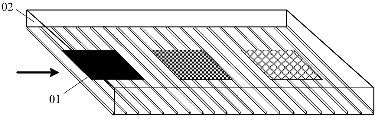
[0034] Due to the over-etching in some parts of the existing developing process during development, it will have a great impact on the display. For example, when a black matrix pattern (Black Matrix, BM for short) is formed by exposure and development processes, a color photoresist pattern such as a red photoresist pattern (R), a green photoresist pattern (G) and a blue photoresist pattern ( In B), because the edge of the black matrix pa...


PUM


Abstract

The embodiments of the invention provide a developing device and a developing method thereof, and photoetching equipment, and relate to the technical field of photolithography, aiming at solving the problem that the uniformity of CD values in a horizontal direction of patterns obtained by means of development of the existing developing device is poorer. The developing device comprises at least onedeveloping chamber, a plurality of spray devices and a transmission device, wherein the plurality of spray devices are distributed in the at least one developing chamber, and are used for spraying developing liquid onto substrates to be developed; the plurality of spray devices respectively spray developing liquid with different concentrations; the transmission device is used for conveying the substrates to be developed so as to enable the substrates to be developed to pass through the position under the plurality of spray devices one by one. The developing device and the developing method thereof are applied in a development process.

Description

technical field [0001] The invention relates to the technical field of photolithography, in particular to a developing device, a developing method thereof, and photolithographic equipment. Background technique [0002] In the production process of display devices, the photolithography process is an important process for forming patterns. The photolithography process includes coating photoresist (Photoresist, referred to as PR glue, also called photoresist), exposure, development and baking. Utilizing the difference in solubility between the photosensitive part and the unphotosensitive part of the PR glue after exposure, use an appropriate solution to dissolve the unphotosensitive part, or on the contrary dissolve the photosensitive part, so that the photoresist material is formed on the surface of the substrate through the photolithography process. Form the required graphics. Photoresist can be divided into positive photoresist and negative photoresist according to its cha...

Claims


Application Information

Patent Timeline
IPC IPC(8): G03F7/30
CPCG03F7/30
Inventor 见帅敏孟维欣郭建解洋徐景华李晓锦孙壮壮
Owner BOE TECH GRP CO LTD
Why Eureka
Try Eureka