Semiconductor x-ray detector
An X-ray and detector technology, applied in the field of semiconductor X-ray detectors, can solve the problems of difficult and impossible production of detectors with a large area and a large number of pixels
- Summary
- Abstract
- Description
- Claims
- Application Information
AI Technical Summary
Problems solved by technology
Method used
Image

Examples
Embodiment Construction
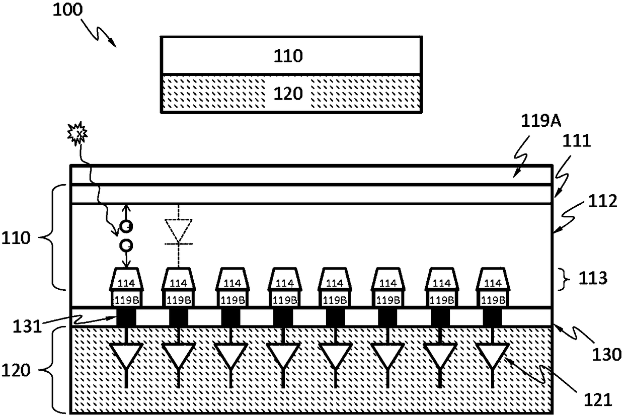
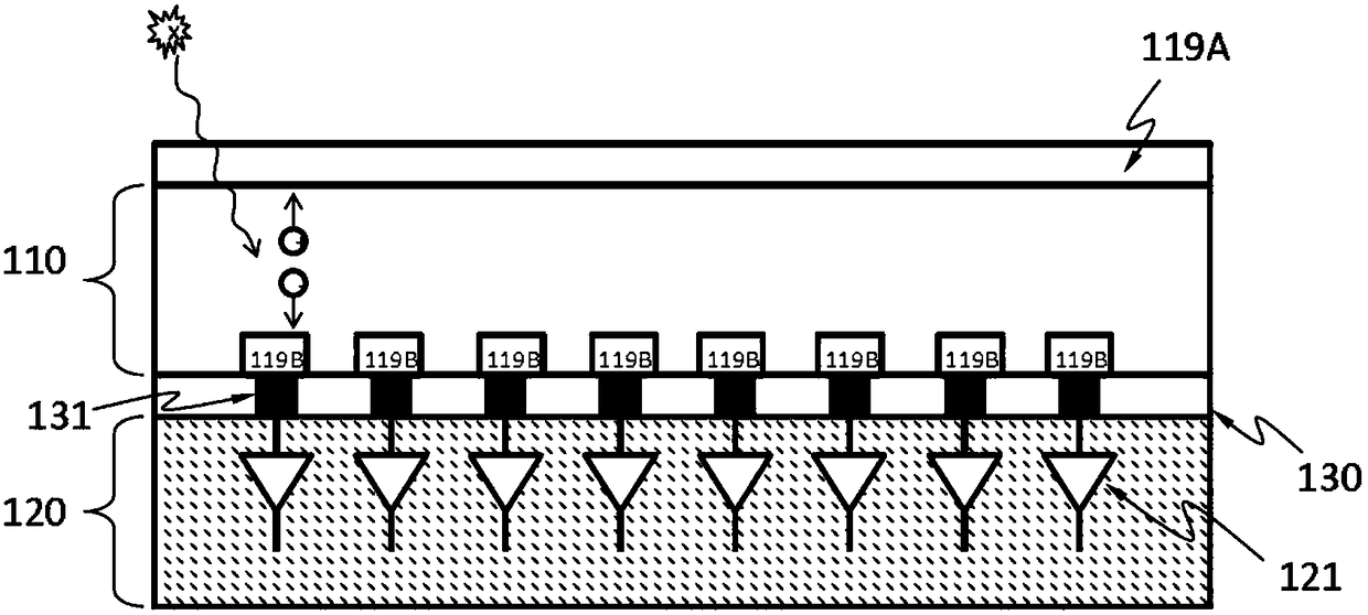
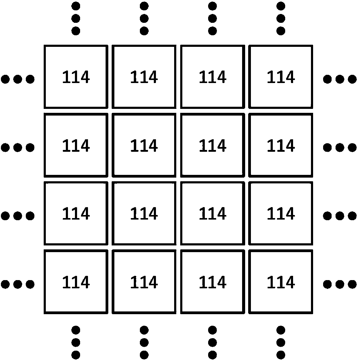
[0063] Figure 1A A semiconductor X-ray detector 100 according to an embodiment is schematically shown. The semiconductor X-ray detector 100 may include an X-ray absorbing layer 110 and an electronic device layer 120 (eg, ASIC) for processing and analyzing electrical signals generated in the X-ray absorbing layer 110 by incident X-rays. In an embodiment, the semiconductor X-ray detector 100 does not include a scintillator. The X-ray absorbing layer 110 may include semiconductor materials such as silicon, germanium, GaAs, CdTe, CdZnTe or combinations thereof. Semiconductors can have high mass attenuation coefficients for x-ray energies of interest. The X-ray absorbing layer 110 may include one or more diodes (eg, p-i-n or p-n) formed from the first doped region 111 , one or more discrete regions 114 of the second doped region 113 . The second doped region 113 may be separated from the first doped region 111 by an (optional) intrinsic region 112 . The discrete portions 114 ar...
PUM
 Abstract
Description
Claims
Application Information
 - R&D Engineer
- R&D Manager
- IP Professional
- Industry Leading Data Capabilities
- Powerful AI technology
- Patent DNA Extraction
Browse by: Latest US Patents, China's latest patents, Technical Efficacy Thesaurus, Application Domain, Technology Topic.
© 2024 PatSnap. All rights reserved.Legal|Privacy policy|Modern Slavery Act Transparency Statement|Sitemap