Non-volatile semiconductor memory device

a non-volatile, semiconductor technology, applied in the direction of transistors, digital storage, instruments, etc., can solve the problems of boosting efficiency, reducing efficiency, and difficult to write. control,

Inactive Publication Date: 2002-09-12
KK TOSHIBA
View PDF0 Cites 164 Cited by
  • Summary
  • Abstract
  • Description
  • Claims
  • Application Information

AI Technical Summary

Benefits of technology

0047] applying a first medium voltage lower than the write voltage and higher than the reference voltage to the control gates of the memory transistors, which being non-selected, intervening between the two memory transisters, which being non-selected; and
0048] applying a second medium voltage lower than the write voltage and higher than the reference voltage to the control gate of at least one of the memory transistors, which being non-selected, on the bit line side from the (K-m)th memory transistor and to the control gate of at least one of the memory transistors, which being non-selected, on the common source line side from the (K+n)th memory transistor.

Problems solved by technology

However, the former system also has a drawback that write control is difficult necessarily because a range of threshold voltages of memory transistors to be used for data recording expands.
For example, in the case of "1" writing, the channel potential of the memory transistor concerned is insufficient, so that wrong writing involving wrong injection of electrons into the floating gate of the memory transistor can occur.
As a result, the boosting efficiency will decrease, which would lead to wrong writing involving electron injection into the floating gate.
A tendency to subdivision has brought about the gate lengths of the memory transistors reaching a gradation of submicrons, which makes it difficult to get a good cutoff characteristic actually.
This causes uneven lengths of the gates due to processing to deteriorate the cutoff characteristic.

Method used


Image

  • Non-volatile semiconductor memory device
  • Non-volatile semiconductor memory device
  • Non-volatile semiconductor memory device

Examples


embodiment 1

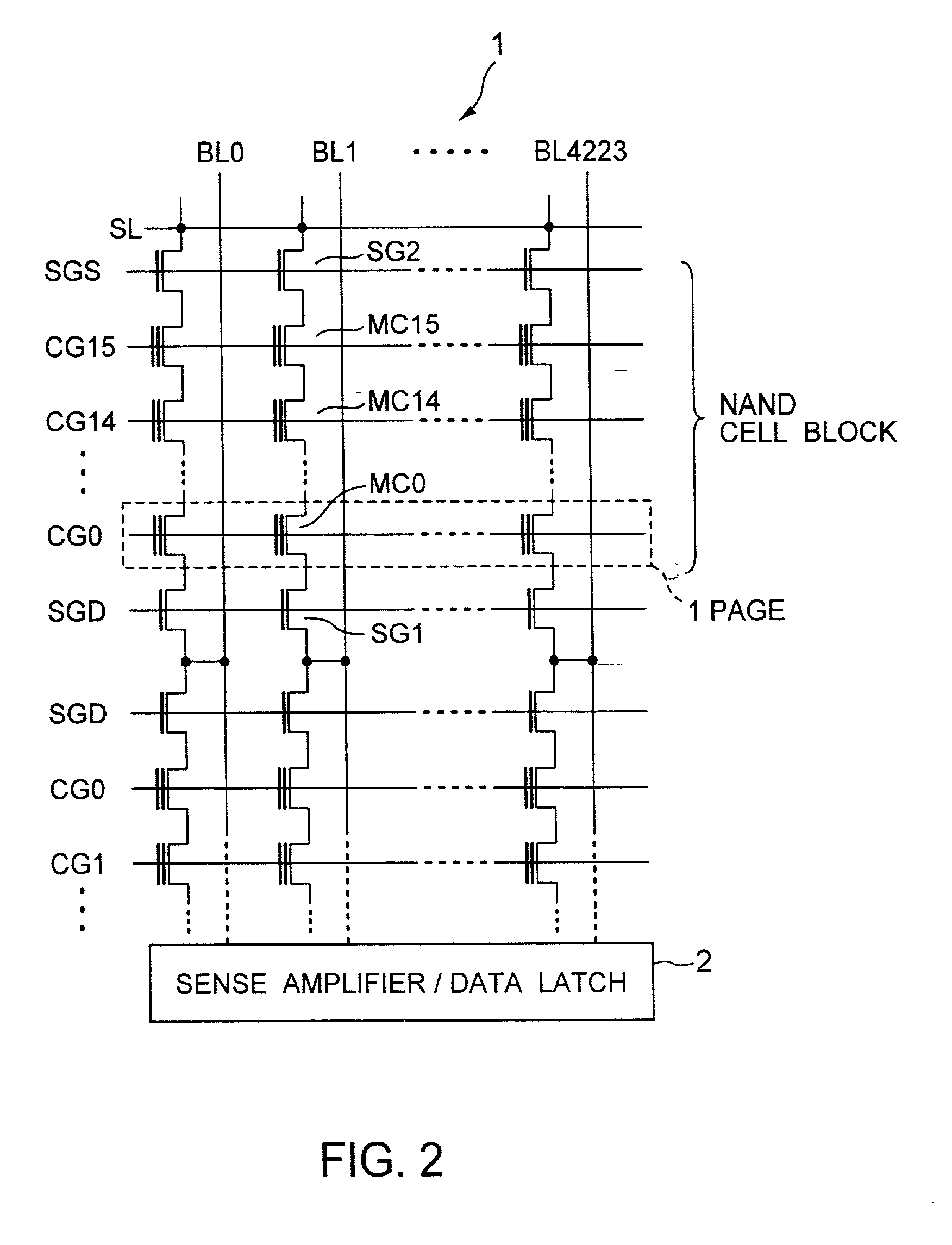
[0069] FIG. 3 shows a relationship among voltages applied to the NAND cells for two bit lines BL0 and BL1 when data is written to second memory transistor from the bit lines BL0 and BL1. FIG. 3 also shows that "0" and "1" data are given to the bit lines BL0 and BL1, respectively.

[0070] Before data writing, old data stored in the NAND cell block is erased collectively. Thus, all the memory transistors of the block are placed in an all-"1" state where the thresholds are low (for example, negative). Then, "0" or "1" write data is given from the sense amplifier / data latch 2 to the bit lines BL and written sequentially into the respective pages of memory transistors, starting with the page nearest to the common source line SL. FIG. 3 also shows that a control gate line CG1 is selected. At this time, before application of the write voltage, Vss=0 V and a boosted voltage Vpre higher than Vdd are given to the bit lines BL0 and BL1, respectively. At this time, by applying Vdd+.alpha. and Vss...

embodiment 2

[0084] In the above embodiment, one medium voltage Vpass was used. For example, in the example of FIG. 3, the medium voltage Vpass applied to the first control gate line CG0 when the second control gate line CG1 from the bit line was selected was an auxiliary voltage to boost as a unit the channel areas of the two memory transistors MC01 and MC11 on the "1" data writing side. For this reason, a specified medium voltage may be, for example, the power supply voltage Vdd or a higher appropriate value as the case may be. In this case, however, it is necessary to prevent no "0" data from being written into a non-selected memory transistor MC00 on the "0" writing bit line BL0 side. In this sense, the medium voltage should be lower than the writing voltage Vpgm.

[0085] In the example of FIG. 3, the medium voltage Vpass to be applied to the control gate lines CG3-CG15 through which the data writing was already performed is different in purpose from that applied to the control gate line CG0. ...

embodiment 3

[0092] In the previous embodiments, the conventional LSB system was basically used in which when "1" data is to be written, the channel of a memory transistor adjacent to the selected memory transistor is turned off. Only when a second memory transistor from each of the bit line and the common source line of the NAND cell were selected, the basic LSB system was modified.

[0093] In contrast, one embodiment in which the basic LSB system itself is modified will be described next. A write mode to be employed in this embodiment is based on the idea that when a control gate line in the NAND cell is selected, a memory transistor that cuts off its channel to boost the channel may not be a memory transistor adjacent to the selected memory transistor, but any two memory transistors between which the selected memory transistor is disposed may be used for that purpose. In this case, a medium voltage needs to be applied to the control gate lines of non-selected memory transistors disposed along w...


PUM


Abstract

A non-volatile semiconductor memory device having a write mode in which wrong writing is prevented surely. The storage device comprises a NAND cell comprising a plurality of memory transistors connected in series and also connected at one end via a select gate transistor CG1 to a bit line BL and at the other end via a select gate transistor SG2 to a common source line SL. A write voltage Vpgm is applied to a control gate of a selected memory transistor in the NAND cell and Vss is applied to the controls gates of non-select memory transistors each adjacent to the selected memory transistor to thereby write data into the select memory transistor. When a second memory transistor from the bit line BL side is selected in the writing operation, a medium voltage Vpass is applied to the control gate of a first non-selected memory transistor from the bit line BL side, and a medium voltage Vpass is applied to the control gates of third and subsequent non-selected memory transistors from the bit line BL side.

Description

CROSS-REFERENCE TO RELATED APPLICATIONS[0001] This application is based upon and claims the benefit of priority from the prior Japanese Patent Application No. 2001-061489, filed on Mar. 6, 2001; entire contents of which are incorporated herein by reference.BACKGROUND OF THE INVENTION[0002] The present invention relates to electrically writable non-volatile semiconductor devices (EEPROMs), and more particularly to an EEPROM employing a NAND type cell array.[0003] In the past, NAND-type flash EEPROMs are known as highly integratable EEPROMs. Memory transistors arranged in rows columns and composing a NAND-type flash EEPROM each have a stacked gate structure of a charge storage layer (a floating gate), formed on a semiconductor substrate through an insulting film, and a control gate. The memory transistors in each row or column are connected in series such that any adjacent transistors share a source and drain diffusion layer. Each string of such series-connected transistors has a pair...

Claims


Application Information

Patent Timeline
Patent Type & Authority Applications(United States)
IPC IPC(8): G11C16/04G11C16/02G11C16/06G11C16/10H01L21/8247H01L27/115H01L29/788H01L29/792
CPCG11C16/0483G11C16/10G11C16/06
Inventor MATSUNAGA, YASUHIKOYAEGASHI, TOSHITAKEARAI, FUMITAKASHIROTA, RIICHIRO
Owner KK TOSHIBA
Why Eureka
Try Eureka