Memory structure and forming method thereof

A technology of memory and storage area, applied in the direction of electric solid-state devices, semiconductor devices, electrical components, etc., can solve the problems of poor read and write ability, low read noise capacity, etc.

Active Publication Date: 2018-07-13
SEMICON MFG INT (SHANGHAI) CORP +1
View PDF3 Cites 3 Cited by
  • Summary
  • Abstract
  • Description
  • Claims
  • Application Information

AI Technical Summary

Problems solved by technology

[0006] However, the memory formed by the prior art still has the disadv

Method used


Image

  • Memory structure and forming method thereof
  • Memory structure and forming method thereof
  • Memory structure and forming method thereof

Examples


Embodiment Construction

[0037] The memory structure of the prior art has many problems, for example, the static noise capacity of the static memory is small, and the anti-interference ability is poor.

[0038] Combining with the memory of the existing technology, the reasons for the small static noise capacity and poor anti-interference ability of the memory are analyzed:

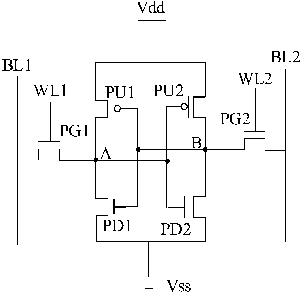
[0039] figure 1 It is a structural diagram of a static memory structure.

[0040] Please refer to figure 1 , the static memory includes: a first pull-up transistor PU1, a first pull-down transistor PD1, a first pass transistor PG1, a second pull-up transistor PU2, a second pull-down transistor PD2 and a second pass transistor PG2. The source of the first pull-up transistor PU2 is connected to the drain of the first pull-down transistor PD1 to form a first storage node A, and the source of the second pull-up transistor PU2 is connected to the drain of the second pull-down transistor PD2 The drains are connected to form a second ...


PUM


Abstract

The invention provides a memory structure and a forming method thereof. The memory structure comprises a first transmission transistor and a second transmission transistor, wherein the first transmission transistor comprises a first transmission drain region and a first transmission source region; the first transmission source region and the first transmission drain region are provided with firstdoped ions; the concentration of the first doped ions in the first transmission drain region is different from that in the first transmission source region; the second transmission transistor comprises a second transmission drain region and a second transmission source region; the second transmission source region and the second transmission drain region are provided with second doped ions; and the concentration of the second doped ions in the second transmission drain region is different from that in the second transmission source region. The writing ability of a memory can be improved whilethe noise reading capacity of the memory is improved.

Description

technical field [0001] The invention relates to the technical field of semiconductor manufacturing, in particular to a memory structure and a forming method thereof. Background technique [0002] With the development of information technology, the amount of stored information has increased dramatically. The increase in the amount of stored information has promoted the rapid development of memory, and at the same time put forward higher requirements for the stability of memory. [0003] A basic Static Random Access Memory (SRAM) relies on six transistors that form two cross-coupled inverters. Each inverter includes: a pull-up transistor, a pull-down transistor and an access transistor. [0004] In order to obtain sufficient anti-interference capability and reading stability, the transistors used to form the memory are mostly Fin Field-Effect Transistors (Fin Field-Effect Transistors, FinFETs). In FinFET transistors, the gate is a 3D structure covering three surfaces of the...

Claims


Application Information

Patent Timeline
IPC IPC(8): H01L27/11
CPCH10B10/12
Inventor 王楠
Owner SEMICON MFG INT (SHANGHAI) CORP
Why Eureka
Try Eureka