Display panel and manufacturing method thereof

A technology for display panels and display areas, which is applied in semiconductor/solid-state device manufacturing, semiconductor devices, electrical components, etc., and can solve problems such as affecting display and film cracks

Active Publication Date: 2018-07-13
BOE TECH GRP CO LTD +1
View PDF5 Cites 40 Cited by
  • Summary
  • Abstract
  • Description
  • Claims
  • Application Information

AI Technical Summary

Problems solved by technology

[0004] Embodiments of the present invention provide a display panel, its manufacturing method and display panel, which are used to solve the problem of cracks in the film layer in the cutting area caused by the impact of laser energy in the prior art when cutting with laser technology, and the cracks are conducted inward into the display area. , a problem that affects the display

Method used


Image

  • Display panel and manufacturing method thereof
  • Display panel and manufacturing method thereof
  • Display panel and manufacturing method thereof

Examples


Embodiment Construction

[0027] In order to make the object, technical solution and advantages of the present invention clearer, the display panel provided by the embodiment of the present invention, its manufacturing method, the organic light-emitting display panel and the specific implementation of the display panel will be described in detail below with reference to the accompanying drawings.

[0028] The film thickness and shape of each layer in the drawings do not reflect the real scale of the display panel, but are only intended to schematically illustrate the content of the present invention.

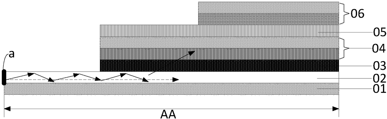
[0029] In the existing technology, such as figure 1 As shown, the flexible OLED display panel includes a base substrate 01, and the base substrate 01 includes a display area and a peripheral area AA, figure 1 Only the peripheral region AA is shown in the figure, the substrate 01 in the peripheral region AA includes a barrier layer 02 completely covering the substrate 01, a buffer layer 03 above the barri...


PUM


Abstract

The invention discloses a display panel and a manufacturing method thereof. The display panel comprises a substrate, the substrate comprises a display area and a surrounding area surrounding the display area, and the display panel further comprises at least one layer of protective layer covering the cutting area corresponding to a cutting line of the surrounding area. The display panel has the advantages that the protective layer is arranged at the edge of the surrounding area, the protective layer can absorb laser energy and release impact force when the laser technology is used subsequentlyfor cutting, edge film layers are prevented from being heated and impacted to generate cracks spreading to the display area, and problems that the film layers of the cutting area is prone to cracks due to excessive laser intensity in the existing technology and the cracks conduct inward into the display area to affect the display are solved.

Description

technical field [0001] The invention relates to the field of display technology, in particular to a display panel and a manufacturing method thereof. Background technique [0002] In the field of display, due to the organic light emitting diode (Organic Light Emitting Display, OLED) display panel has self-illumination, no backlight, high contrast, thin thickness, wide viewing angle, fast response speed, can be used for flexible panels, operating temperature Wide range and other excellent characteristics are considered to be the new application technology of the next generation of flat panel displays. At present, flexible OLED display devices have become an important development direction of display devices. [0003] In the prior art, the manufacturing process of the flexible display panel is as follows: multiple flexible display panels are formed on a large display motherboard, and then cut to form independent flexible display panels. At present, flexible OLEDs are cut by ...

Claims


Application Information

Patent Timeline
Patent Type & Authority Applications(China)
IPC IPC(8): H01L51/52H01L51/56H01L27/32
CPCH10K59/12H10K50/844H10K71/00
Inventor 王格蒋志亮刘建志常程
Owner BOE TECH GRP CO LTD
Why Eureka
Try Eureka