Unlock instant, AI-driven research and patent intelligence for your innovation.

Method of recognizing wafer

一种识别方法、识别设备的技术,应用在微电子领域,能够解决污染、不良保护层、区域缺陷等问题

Inactive Publication Date: 2018-07-20
NAN YA TECH
View PDF3 Cites 0 Cited by
  • Summary
  • Abstract
  • Description
  • Claims
  • Application Information

AI Technical Summary

Problems solved by technology

For example, foreign particle contamination or other contamination, area defects, or poor protective layers may occur on the wafer

Method used


Image

  • Method of recognizing wafer
  • Method of recognizing wafer
  • Method of recognizing wafer

Examples


Embodiment Construction

[0076] Embodiments, or examples, of the present disclosure shown in the drawings will now be described using specific language. It should be understood that no limitation of the scope of the present disclosure is thereby intended. Any alterations and modifications to the described embodiments, and any further application of the principles described in this document are deemed to be as would normally occur to one skilled in the art to which this disclosure pertains. Reference numbers may be repeated throughout embodiments, but this does not necessarily mean that the feature(s) of one embodiment need to be applied to another embodiment, even if they share the same reference number.

[0077] It will be understood that when an element is referred to as being "connected to" or "coupled to" another element, it can be directly connected or coupled to the other element or intervening elements may be present.

[0078] It should be understood that although the terms first, second, thir...


PUM


Abstract

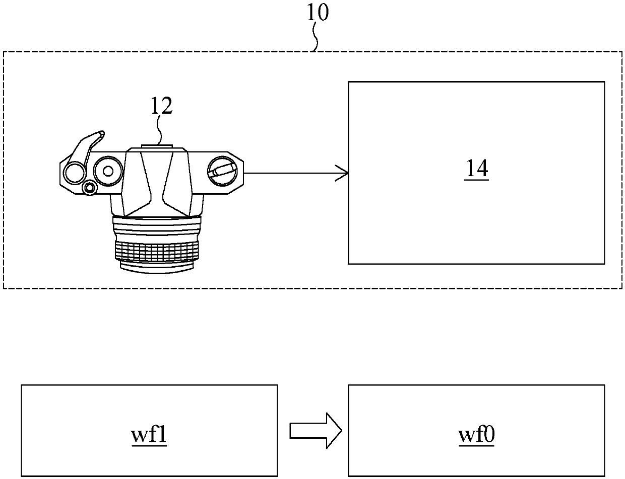
The present invention discloses a method and a device for recognizing a wafer. The method includes the steps of: obtaining image information including a first vector by capturing an image of a first wafer, wherein the first wafer is known to be a good product; obtaining image information including a second vector by capturing an image of a second wafer, wherein the second wafer is known to be a defective product; calculating a projection vector based on a covariance matrix associated with the first vector and the second vector; obtaining image information including a third vector by capturingan image of a third wafer under a test; projecting each of the first vector, the second vector and the third vector onto the projection vector; and classifying the third wafer as either the good product or the defective product based on the projected first vector, the projected second vector and the projected third vector. The method and the device for recognizing a wafer can improve the recognition rate of a bad wafer.

Description

technical field [0001] The present disclosure relates to the technical field of microelectronics, and in particular, to a wafer identification method and equipment. Background technique [0002] Wafers are generally used as the basis for constructing semiconductor devices. During the process of manufacturing semiconductor devices, wafers may be damaged. For example, foreign particle contamination or other contamination, area defects, or poor protective layers may occur on the wafer. [0003] The Discussion section of this Background Art provides background data only. Statements in this Background discussion are not an admission that the subject matter disclosed in this section constitutes prior art to the present disclosure, and no part of this section is intended to be taken as an admission that any part of this application, including this Background section, constitutes prior art to the present disclosure. Contents of the invention [0004] An embodiment of the prese...

Claims


Application Information

Patent Timeline
Patent Type & Authority Applications(China)
IPC IPC(8): G06K9/00G06K9/62G06V10/764
CPCG06V20/30G06F18/24G06T7/001G06T2207/30148G06V10/764G06V10/7715G06F18/2135G06F18/24147
Inventor 方伟力
Owner NAN YA TECH