Pixel circuit and driving method thereof, electroluminescent display panel and display device

A technology of pixel circuits and light-emitting modules, applied in static indicators, instruments, etc., can solve problems such as poor display, driving thin-film transistor T2 threshold voltage shift, and organic light-emitting diode D brightness changes, etc., to eliminate poor display and avoid voltage Stable and stable effect

Active Publication Date: 2018-07-27
HEFEI XINSHENG OPTOELECTRONICS TECH CO LTD +1
5 Cites 13 Cited by

AI-Extracted Technical Summary

Problems solved by technology

[0004] However, because the driving thin film transistor T2 in the pixel circuit is under the action of the gate bias for a long time, the threshold voltage of the d...

Method used

In the above-mentioned pixel circuit provided by the embodiment of the present invention, in the first frame, the first gate of the double-gate thin film transistor Td is in the working state, and in the adjacent second frame, the double-gate thin film transistor Td For example, when the second gate is in the working state, the threshold voltage shift of the first gate of the double-gate thin film transistor Td is =k1×│Vdata1│β1tγ1, k1 is a constant, and the threshold voltage shift of the second gate is =k2×│Vdata2│β2tγ2, k2 is a constant; the bias voltage of the first gate in the first frame and the bias voltage of the second gate in the second frame have opposite effects on the TFT channel, therefore, in the two frames After the signal loading is completed, the threshold voltage shift is k1×│Vdata1│β1tγ1-k2×│Vdata2│β2tγ2; specifically, parameters such as β and γ can be made consistent through process adjustment, that is, data1 and data2 are equal, so that in two frames After the signal loading is completed, the threshold voltage drift is as close to 0 as possible, so that due to the alternate operation of the first gate and the second gate, the threshold voltage drift of a group of odd and even frames cancels each other, avoiding the electrical characteristics of the thin film transistor. coming brightness changes.
[0077] Thereafter, until the next t1 stage occurs, that is, when the first gate line signal terminal Gate1 inputs the gate line scanning signal again, the first thin film transistor T1 is in the state of working conduction, while the second thin film transistor T2 is in the off state. Therefore, using the alternate operation of the first thin film transistor T1 and the second thin film transistor T2, and then driving the alternate operation of the first gate and the second gate of the double-gate thin film transi...

Abstract

The invention discloses a pixel circuit and a driving method thereof, an electroluminescent display panel and a display device. The pixel circuit comprises a first switch module, a second switch module, a light-emitting module and a dual-driving module. On the basis of improvement of the pixel circuit, a first drive end of the dual-driving module is connected with a first node and a second drive end is connected with a second node. When a first grid line signal terminal and a second grid line signal terminal input grid line scanning signal alternately, the first switch module and the second switch module works alternately and thus the first drive end and the second drive end of the dual-driving module works alternately, so that the light-emitting module is driven to emit light. Therefore,because of the alternate work of the two drive ends, a phenomenon of high voltage instability caused by the long-term working state of one drive end of the dual-driving module is avoided, so that thestability of the pixel grayscale brightness is ensured and the poor displaying is eliminated.

Application Domain

Technology Topic

Image

  • Pixel circuit and driving method thereof, electroluminescent display panel and display device
  • Pixel circuit and driving method thereof, electroluminescent display panel and display device
  • Pixel circuit and driving method thereof, electroluminescent display panel and display device

Examples

  • Experimental program(1)

Example Embodiment

[0036] Specific implementations of a pixel circuit, a driving method thereof, an electroluminescence display panel, and a display device provided by embodiments of the present invention will be described in detail below with reference to the accompanying drawings.
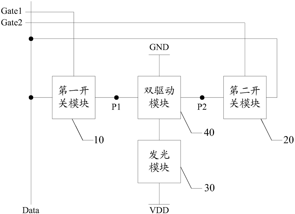
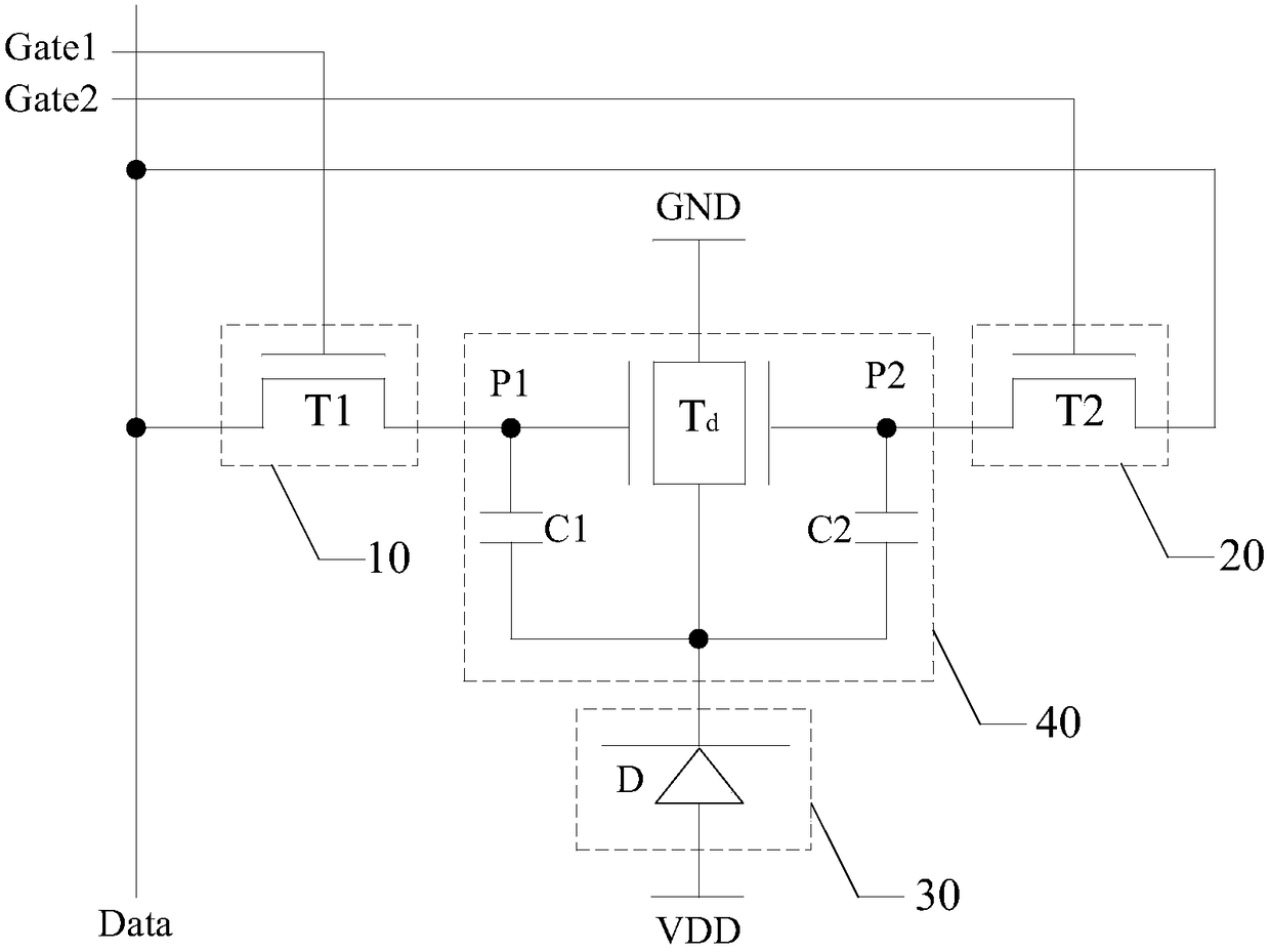
[0037] The embodiment of the present invention provides a pixel circuit, such as figure 2 As shown, it may include: a first switch module 10, a second switch module 20, a light-emitting module 30, and a dual drive module 40; wherein,
[0038] The signal control end of the first switch module 10 is connected to the first gate line signal end Gate1, the signal input end is connected to the data line signal end Data, and the signal output end is connected to the first node P1; Under the control of the gate line scan signal input by the gate line signal terminal Gate1, the data signal provided by the data line signal terminal Data is transmitted to the first node P1;
[0039]The signal control terminal of the second switch module 20 is connected to the second gate line signal terminal Gate2, the signal input terminal is connected to the data line signal terminal Data, and the signal output terminal is connected to the second node P2; Under the control of the gate line scan signal input by the gate line signal terminal Gate2, the data signal provided by the data line signal terminal Data is transmitted to the second node P2;
[0040] The first driving terminal of the dual driving module 40 is connected to the first node P1, the second driving terminal is connected to the second node P2, the signal input terminal is connected to the first reference signal terminal GND, and the signal output terminal is connected to the first terminal of the light emitting module 30 connected; the second terminal of the light emitting module 30 is connected to the second reference signal terminal VDD; the dual driving module 40 is used to drive the light emitting module 30 to emit light under the control of the potential of the first node P1 or the second node P2.
[0041] In the pixel circuit provided by the embodiment of the present invention, by improving the pixel circuit, the first driving end of the dual driving module 40 is connected to the first node P1, the second driving end is connected to the second node P2, and the first gate line When the signal terminal Gate1 and the second gate line signal terminal Gate2 alternately input the gate line scanning signal, the first switch module 10 and the second switch module 20 work alternately, so that the first drive terminal and the second drive terminal of the dual drive module 40 alternately work, so as to drive the light-emitting module 30 to emit light; in this way, through the alternate operation of the two driving terminals, the voltage instability caused by one driving terminal of the dual-driving module 40 being in the working state for a long time is avoided, and the stability of the gray-scale brightness of the pixel is guaranteed. performance, eliminating poor display.
[0042] During specific implementation, in order to illustrate more clearly that the two driving terminals of the dual driving module 40 work alternately, in the above-mentioned pixel circuit provided by the embodiment of the present invention, as image 3 As shown, the dual driver module 40 may specifically include: a double-gate thin film transistor Td, a first capacitor C1, and a second capacitor C2; wherein,
[0043] The first gate of the double-gate thin film transistor Td is connected to the first node P1, the second gate is connected to the second node P2, the source is connected to the first reference signal terminal GND, and the drain is connected to the first terminal of the light emitting module 30 ;
[0044] The first capacitor C1 is connected between the first node P1 and the first end of the light emitting module 30;
[0045] The second capacitor C2 is connected between the second node P2 and the first end of the light emitting module 30 .
[0046] Specifically, the working principle of the dual-gate thin film transistor Td suppressing the threshold voltage drift can be described according to the following empirical formula of the threshold voltage drift of the thin film transistor:
[0047] ΔV th ∝│V gate │ β t γ
[0048] Among them, ΔV th Indicates the shift amount of the threshold voltage, V gate Represents gate voltage, t represents time, β and γ represent constants related to the characteristics of the thin film transistor itself.
[0049] In the above pixel circuit provided by the embodiment of the present invention, in the first frame, the first gate of the double-gate thin film transistor Td is in the working state, and in the adjacent second frame, the second gate of the double-gate thin film transistor Td For example, when the gate is in the working state, the threshold voltage shift of the first gate of the double-gate thin film transistor Td is =k1×│V data1 │ β1 t γ1 , k1 is a constant, the threshold voltage shift of the second gate is =k2×│V data2 │ β2 t γ2 , k2 is a constant; the bias voltage of the first gate in the first frame and the bias of the second gate in the second frame have opposite effects on the channel of the thin film transistor. Therefore, after the signal loading of the two frames is completed, the threshold voltage The drift is k1×│V data1 │ β1 t γ1 -k2×│V data2 │ β2 t γ2; Specifically, parameters such as β and γ can be made consistent through process adjustment, that is, data1 and data2 are equal, so that the threshold voltage drift is as close to 0 as possible after the signal loading of the two frames is completed, so that due to the first gate and the second Alternate operation of the gate makes the threshold voltage shifts of a group of odd and even frames offset each other, avoiding brightness changes caused by changes in the electrical characteristics of the thin film transistors.
[0050] Of course, the alternate operation of the first gate and the second gate of the double-gate thin film transistor Td is not limited to being performed in two connected frames, but can also be performed in different frames at intervals, which is not limited here.
[0051] Specifically, the data signal provided by the data line signal terminal Data is a high-level signal, and the double-gate thin film transistor Td is an N-type thin film transistor; or, the data signal provided by the data line signal terminal Data is a low-level signal, and the double-gate thin film transistor Td is a low-level signal. Td is a P-type thin film transistor.
[0052] The above is only an example to illustrate the specific structure of the dual-drive module 40. In actual implementation, the specific structure of the dual-drive module 40 is not limited to the above-mentioned structure provided by the embodiment of the present invention, and may also be other structures known to those skilled in the art. Here I won't go into details.
[0053] Specifically, in the above pixel circuit provided by the embodiment of the present invention, the double-gate thin film transistor Td is a P-type thin film transistor, and the anode of the light emitting module 30 is connected to the drain of the double-gate thin film transistor Td; or, when the double-gate thin film transistor Td It is an N-type thin film transistor, and the cathode of the light emitting module 30 is connected to the drain of the double-gate thin film transistor Td.
[0054] When the double-gate thin film transistor Td is a P-type thin film transistor, the first terminal of the light emitting module 30 is a positive pole, and the second terminal is a negative pole. The first reference signal terminal is a high-level voltage terminal, such as voltage VDD, and the second reference signal terminal is a low-level voltage terminal, for example, the voltage may be ground GND or VSS.
[0055] When the double-gate thin film transistor Td is an N-type thin film transistor, the first terminal of the light emitting module 30 is a negative pole, and the second terminal is a positive pole. The first reference signal terminal is a low-level voltage terminal, for example, the voltage may be ground GND or VSS, and the second reference signal terminal is a high-level voltage terminal, for example, the voltage may be VDD. Among them, VDD>GND>VSS.
[0056] In specific implementation, in the above-mentioned pixel circuit provided by the embodiment of the present invention, as image 3 As shown, the first switch module 10 may include: a first thin film transistor T1; wherein,
[0057] The gate of the first thin film transistor T1 is connected to the first gate line signal terminal Gate1, the source is connected to the data line signal terminal Data, and the drain is connected to the first node P1.
[0058] Specifically, the first thin film transistor T1 transmits the data signal provided by the data line signal terminal Data to the first node P1 under the control of the gate scan signal input from the first gate signal terminal Gate1.
[0059] Further, the gate scan signal input by the first gate signal terminal Gate1 is a high-level signal, and the first thin film transistor T1 is an N-type thin film transistor; or, the gate scan signal input by the first gate signal terminal Gate1 is low Level signal, the first thin film transistor T1 is a P-type thin film transistor.
[0060] The above is only an example to illustrate the specific structure of the first switch module 10. In actual implementation, the specific structure of the first switch module 10 is not limited to the above-mentioned structure provided by the embodiment of the present invention, and may also be other structures known to those skilled in the art. I won't go into details here.
[0061] In specific implementation, in the above-mentioned pixel circuit provided by the embodiment of the present invention, as image 3 As shown, the second switch module 20 may include: a second thin film transistor T2; wherein,
[0062] The gate of the second thin film transistor T2 is connected to the second gate line signal terminal Gate2, the source is connected to the data line signal terminal Data, and the drain is connected to the second node P2.
[0063] Specifically, the second thin film transistor T2 transmits the data signal provided by the data line signal terminal Data to the second node P2 under the control of the gate scan signal input from the second gate signal terminal Gate2.
[0064] Further, the gate scan signal input by the second gate signal terminal Gate2 is a high-level signal, and the second thin film transistor T2 is an N-type thin film transistor; or, the gate scan signal input by the second gate signal terminal Gate2 is low Level signal, the second thin film transistor T2 is a P-type thin film transistor.
[0065] The above is only an example to illustrate the specific structure of the second switch module 20. In actual implementation, the specific structure of the second switch module 20 is not limited to the above-mentioned structure provided by the embodiment of the present invention, and may also be other structures known to those skilled in the art. I won't go into details here.
[0066] Of course, the transistors involved in the above-mentioned pixel circuit provided by the embodiment of the present invention are not limited to thin film transistors (Thin Film Transistor, TFT), and may also be Metal Oxide Semiconductor Field Effect Transistors (Metal Oxide Semiconductor, MOS); and, The source and drain of the above thin film transistors (including the first thin film transistor T1, the second thin film transistor T2, and the double-gate thin film transistor Td) have the same manufacturing process, and the names are interchangeable, which can be determined according to the direction of the voltage Change in name.
[0067] In specific implementation, in order to realize light emission, in the above-mentioned pixel circuit provided by the embodiment of the present invention, as image 3 As shown, the light emitting module 30 may include: an organic light emitting diode D; wherein,
[0068] The first terminal of the organic light emitting diode D is connected to the signal output terminal of the dual driving module 40 , and the second terminal is connected to the second reference signal terminal VDD.
[0069] Of course, the organic light emitting diode D involved in the above pixel circuit provided by the embodiment of the present invention is an active matrix electroluminescent device, so it is not limited to the organic light emitting diode, and may also be a quantum dot light emitting diode.
[0070] It should be noted that the improvement to the pixel circuit provided by the embodiment of the present invention is not limited to figure 2 and image 3 The illustrated structure of the pixel circuit may also be a pixel circuit with other structure, which is not limited here.
[0071] Combine below image 3 The pixel circuit shown and Figure 4 The working sequence diagram of the pixel circuit shown is a description of the working process of the above-mentioned pixel circuit provided by the embodiment of the present invention.
[0072] like Figure 4 As shown, it is the timing diagram of the pixel circuit provided in this embodiment, each frame in two consecutive frames can be divided into two time periods; image 3 In the pixel circuit shown, it is assumed that each thin film transistor is an N-type thin film transistor, the voltage of the first reference signal terminal is ground GND, and the voltage of the second reference signal terminal is VDD.
[0073] In the stage t1, the first gate line signal terminal Gate1 inputs the gate line scanning signal, the first thin film transistor T1 is turned on, and transmits the data signal VData1 provided by the data line signal terminal Data to the first node P1, and at the same time charges the first capacitor C1 ; At this time, the first grid of the double-gate thin film transistor Td is turned on, and the voltage of the negative pole of the organic light emitting diode D is kept at a low level. Because the voltage of the positive pole of the organic light emitting diode D is a high level voltage VDD, the organic light emitting diode is driven The light emitting diode D emits light.
[0074] In stage t2, the first gate line signal terminal Gate1 stops inputting the gate line scan signal, the first thin film transistor T1 is turned off, the first capacitor C1 starts to discharge at this time, the first gate of the double gate thin film transistor Td continues to conduct, and continues to The voltage of the negative electrode of the organic light emitting diode D is kept at a low level, so that the organic light emitting diode D continues to be driven to emit light.
[0075] In stage t3, the gate line scan signal is input to the second gate line signal terminal Gate2, the second thin film transistor T2 is turned on, the data signal VData2 provided by the data line signal terminal Data is transmitted to the second node P2, and the second capacitor C2 is charged at the same time ; At this time, the second gate of the double-gate thin film transistor Td is turned on, thus driving the organic light emitting diode D to emit light.
[0076] In the stage t4, the second gate line signal terminal Gate2 stops inputting the gate line scan signal, the second thin film transistor T2 is turned off, the second capacitor C2 starts to discharge at this time, the second gate of the double gate thin film transistor Td continues to conduct, and continues to The voltage of the negative electrode of the organic light emitting diode D is kept at a low level, so that the organic light emitting diode D continues to be driven to emit light.
[0077] Thereafter, until the occurrence of the next t1 stage, that is, when the first gate line signal terminal Gate1 inputs the gate line scan signal again, the first thin film transistor T1 is in a working on state, and the second thin film transistor T2 is in an off state; Therefore, the alternate work of the first thin film transistor T1 and the second thin film transistor T2 is used to drive the alternate work of the first gate and the second gate of the double-gate thin film transistor Td, avoiding the possibility of a gate being in the working state for a long time. The resulting threshold voltage drift ensures the stability of pixel grayscale brightness and eliminates poor display.
[0078] Based on the same inventive concept, an embodiment of the present invention also provides a method for driving the above-mentioned pixel circuit provided by an embodiment of the present invention, which may include:
[0079] When the gate line scan signal is input to the first gate line signal terminal, the first switch module transmits the data signal provided by the data line signal terminal to the first node under the control of the gate line scan signal input from the first gate line signal terminal; When the potential of the first node is the potential of the data signal provided by the signal terminal of the data line, the dual driving module drives the light-emitting module to emit light;
[0080] When the gate line scan signal is input to the second gate line signal terminal, the second switch module transmits the data signal provided by the data line signal terminal to the second node under the control of the gate line scan signal input from the second gate line signal terminal; When the potential of the second node is the potential of the data signal provided by the signal terminal of the data line, the dual driving module drives the light-emitting module to emit light.
[0081] Based on the same inventive concept, an embodiment of the present invention also provides an electroluminescent display panel, which may include at least one of the pixel circuits provided in the embodiments of the present invention. For the specific implementation, please refer to the description of the pixel circuits provided in the embodiments of the present invention. The similarities will not be repeated here.
[0082] The embodiment of the present invention also provides a display device, which may include the electroluminescent display panel provided in the embodiment of the present invention, and the display device may be: a mobile phone, a tablet computer, a TV, a monitor, a notebook computer, a digital photo frame, a navigation Any product or component with display function, such as instrument. For the implementation of the display device, reference may be made to the above-mentioned embodiments of the electroluminescent display panel, and repeated descriptions will not be repeated.
[0083] Embodiments of the present invention provide a pixel circuit, a driving method thereof, an electroluminescent display panel, and a display device. The pixel circuit includes a first switch module, a second switch module, a light-emitting module, and a dual drive module. The first drive end is connected with the first node, the second drive end is connected with the second node, the signal input end is connected with the first reference signal end, the signal output end is connected with the first end of the light emitting module; the second end of the light emitting module is connected with the first reference signal end. The second reference signal terminal is connected; the dual driving module is used to drive the light-emitting module to emit light under the potential control of the first node or the second node; therefore, through the improvement of the pixel circuit, the first driving terminal of the dual driving module is A node is connected, and the second driving terminal is connected to the second node. When the gate line scanning signal is input alternately between the first gate line signal terminal and the second gate line signal terminal, the first switch module and the second switch module work alternately, thereby making the The first drive end and the second drive end of the dual drive module work alternately, so as to drive the light emitting module to emit light; in this way, through the alternate work of the two drive ends, it is avoided that one drive end of the dual drive module is in a working state for a long time. The voltage is unstable, which ensures the stability of pixel grayscale brightness and eliminates poor display.
[0084] It will be apparent to those skilled in the art that various modifications and variations can be made in the present invention without departing from the spirit and scope of the invention. Thus, provided that these modifications and variations of the present invention fall within the scope of the claims of the present invention and their equivalents, the present invention is also intended to include these modifications and variations.

PUM

no PUM

Description & Claims & Application Information

We can also present the details of the Description, Claims and Application information to help users get a comprehensive understanding of the technical details of the patent, such as background art, summary of invention, brief description of drawings, description of embodiments, and other original content. On the other hand, users can also determine the specific scope of protection of the technology through the list of claims; as well as understand the changes in the life cycle of the technology with the presentation of the patent timeline. Login to view more.

Similar technology patents

Folding desk lamp used on computer desk

Owner:SUZHOU KUNK & SAM LIGHTING TECH CO LTD

Classification and recommendation of technical efficacy words

  • Avoid voltage instability
  • Guaranteed stability
Why Eureka
Try Eureka