Image sensor, electronic device and image processing method

An image sensor and pixel technology, applied in the field of image processing, can solve problems such as power supply noise cannot be eliminated, and achieve the effects of improving accuracy, realizing analysis, and eliminating power supply noise

Active Publication Date: 2020-03-31
BYD SEMICON CO LTD
View PDF5 Cites 0 Cited by
  • Summary
  • Abstract
  • Description
  • Claims
  • Application Information

AI Technical Summary

Problems solved by technology

[0003] However, the disadvantage of the related technology is that the power supply noise caused by the inconsistency of the power supply of the pixel array cannot be eliminated

Method used


Image

  • Image sensor, electronic device and image processing method
  • Image sensor, electronic device and image processing method
  • Image sensor, electronic device and image processing method

Examples


Embodiment Construction

[0024] Embodiments of the present invention are described in detail below, examples of which are shown in the drawings, wherein the same or similar reference numerals designate the same or similar elements or elements having the same or similar functions throughout. The embodiments described below by referring to the figures are exemplary and are intended to explain the present invention and should not be construed as limiting the present invention.

[0025] An image sensor, an electronic device, and an image processing method according to embodiments of the present invention will be described below in conjunction with the accompanying drawings.

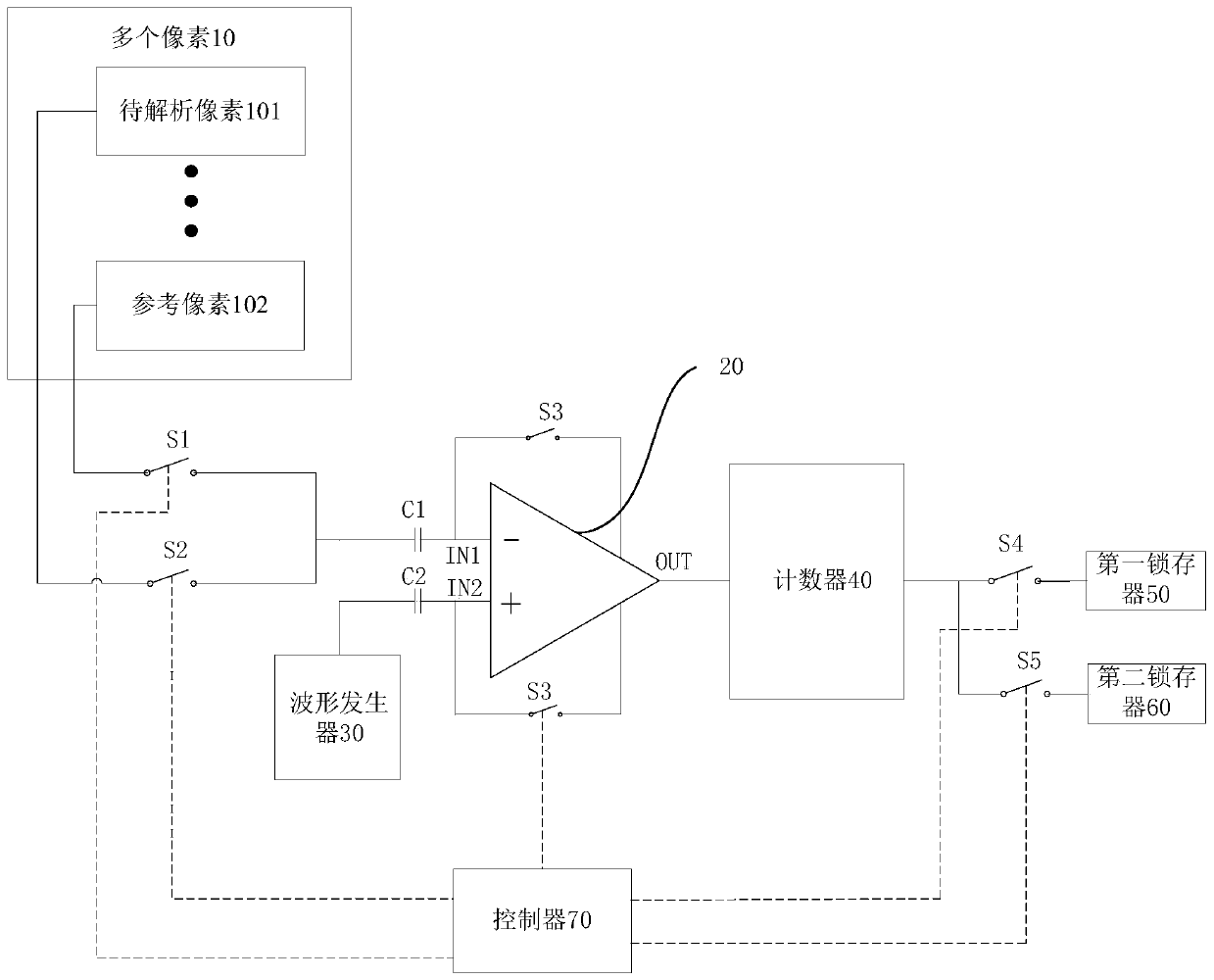
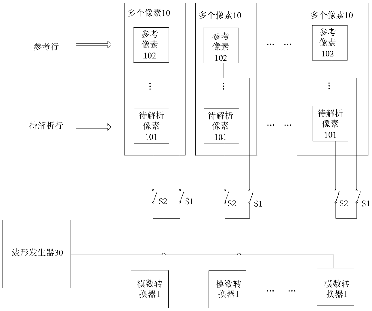
[0026] figure 1 is a schematic block diagram of an image sensor according to an embodiment of the present invention. Such as figure 1 As shown, the image sensor of the embodiment of the present invention includes: a plurality of pixels 10 , a comparator 20 , a waveform generator 30 , a counter 40 , a first latch 50 , a second latch...


PUM


Abstract

The invention discloses an image sensor, which includes: a plurality of pixels, including a pixel to be resolved and a reference pixel; The switch is connected with the reference pixel and the pixel to be resolved, and the comparator also includes a third switch connected between its first input terminal and output terminal, and between the second input terminal and the output terminal; a waveform generator, which communicates with the The second input terminal of the comparator is connected; the counter, its input terminal is connected with the output terminal of the comparator; the first latch and the second latch, the first latch is connected with the output terminal of the counter through the fourth switch, The second latch is connected to the output terminal of the counter through the fifth switch; the controller is used to control the first switch to the fifth switch to generate a conversion result according to the Reset signal and the Signal signal output by the pixel to be analyzed and the reference pixel, thereby The power supply noise of the pixel array can be effectively eliminated, and the analysis precision is improved.

Description

technical field [0001] The invention relates to the technical field of image processing, in particular to an image sensor, an electronic device and an image processing method. Background technique [0002] Image sensors (CMOS image sensors, CIS) have been more and more widely used due to the advantages of low power consumption and the ability to integrate sensors and readout circuits on the same chip. The image sensor in the related art is generally composed of a pixel (pixel) array and a corresponding readout circuit. Due to the existence of metal wiring parasitics, in practical applications, the power supply of each column is inconsistent, which causes the difference between columns, that is, Power supply noise is generated, wherein the power supply noise may include power supply noise caused by inconsistent power supply of the pixel array and power supply noise caused by inconsistent power supply of the readout circuit. [0003] However, the disadvantage of the related t...

Claims


Application Information

Patent Timeline
Patent Type & Authority Patents(China)
IPC IPC(8): H04N5/357H04N5/374
CPCH04N25/60H04N25/76
Inventor 裴学用郭先清
Owner BYD SEMICON CO LTD
Why Eureka
Try Eureka