Eureka AIR delivers breakthrough ideas for toughest innovation challenges, trusted by R&D personnel around the world.

Stacked silicon package assembly with stiffener

A reinforcement and component technology, applied in semiconductor/solid-state device parts, electrical components, semiconductor devices, etc., can solve problems such as welding connection failure, impact, damage, etc.

Active Publication Date: 2021-12-07
XILINX INC
View PDF9 Cites 0 Cited by
  • Summary
  • Abstract
  • Description
  • Claims
  • Application Information

AI Technical Summary

Problems solved by technology

However, especially in larger chip package assemblies, the stiffeners themselves may bend or twist, or even delaminate from the package substrate, thus still allowing undesired warping and bowing to occur during manufacturing and / or use
This warping and bowing of the package substrate can lead to failure of solder connections or other damage to components and devices of the chip package assembly, which can adversely affect device performance and reliability

Method used


Image

  • Stacked silicon package assembly with stiffener
  • Stacked silicon package assembly with stiffener
  • Stacked silicon package assembly with stiffener

Examples


Embodiment Construction

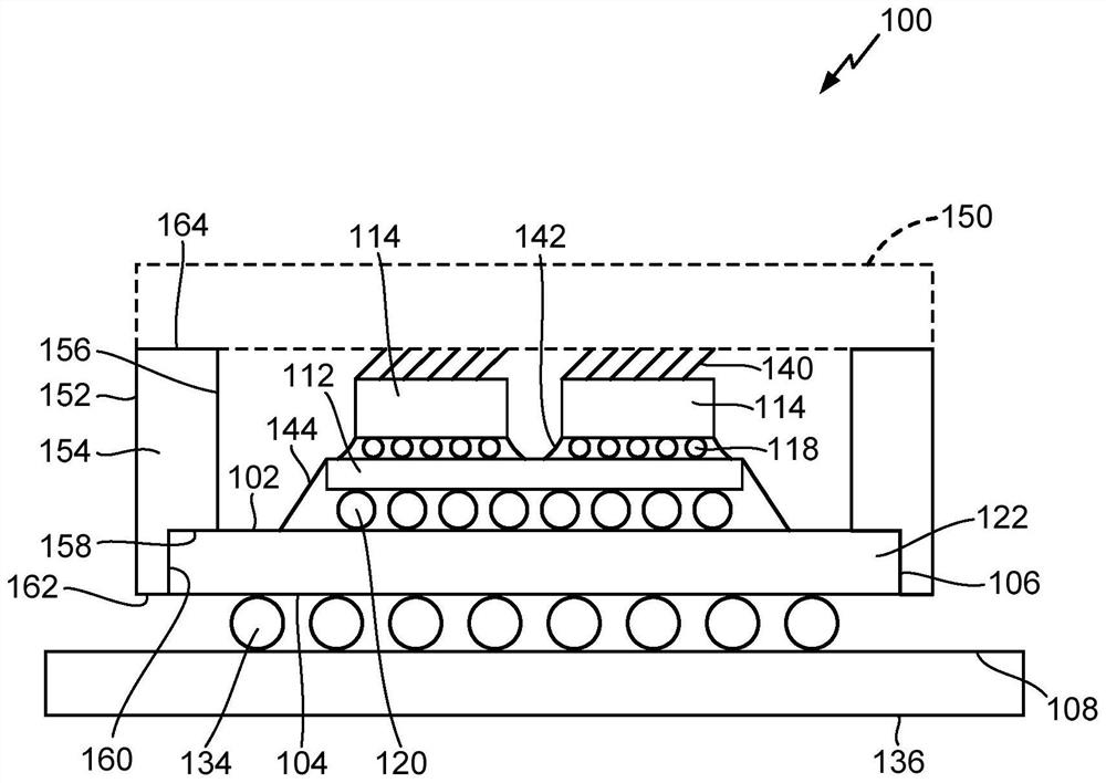
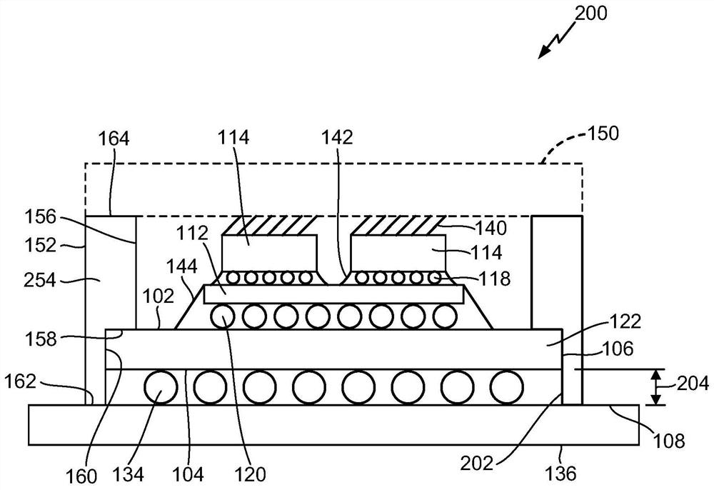
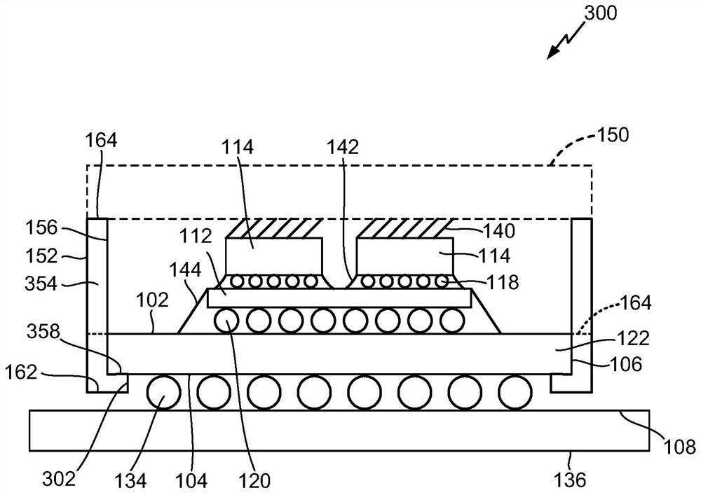
[0035] Chip package assemblies utilizing improved stiffeners and methods of manufacturing the same are provided. A chip package assembly as described herein includes at least one integrated circuit (IC) die and a stiffener disposed on a package substrate. The stiffener is configured to increase the package substrate's resistance to out-of-plane deformation during manufacture and use of the chip package assembly. Advantageously, the increased stiffness of the chip package assembly improves reliability and performance. In various examples described herein, one or more advantages may be realized, including stiffening the package substrate in both the horizontal and vertical axes, a larger adhesive attachment area to reduce delamination, Advantages such as more space for circuit components for chip capacitors, thinner package outlines, and ball grid array (BGA) standoff height control.

[0036] Watch now figure 1 , which schematically shows the integrated chip package assembly...


PUM


Abstract

A chip package assembly (100, 200, 300, 400) utilizing a stiffener (154, 254, 454, 500, 710, 810, 1110) to improve a package substrate (122) to prevent out-of-plane deformation and A method (1400) for manufacturing the chip package assembly. In one example, a chip package assembly is provided that includes a package substrate, at least one integrated circuit (IC) die (114), and a stiffener. The packaging substrate has a first surface (102) and a second surface (104) coupled by a sidewall (106). The at least one IC die is disposed on the first surface of the packaging substrate. A stiffener is disposed on the exterior of the at least one IC die. The stiffener has a first surface (160) disposed outside the sidewall of the package substrate and combined with the sidewall. The stiffener has a second surface (158, 358) bonded to at least one of the first and second surfaces (102, 104) of the package substrate.

Description

technical field [0001] Embodiments of the present application relate generally to chip package assemblies, and more particularly to chip package assemblies that include at least one integrated circuit (IC) die disposed on a package substrate and stiffeners that stiffen the package substrate without out-of-plane deformation. Background technique [0002] Electronic devices such as tablets, computers, copiers, digital cameras, smart phones, control systems, and ATMs often employ electronic components that utilize chip-package components for improved functionality and higher component density. Traditional chip packaging schemes typically utilize a packaging substrate, often combined with a through-silicon via (TSV) interposer, to enable multiple integrated circuit (IC) die to be mounted on a single packaging substrate. An IC die may include memory, logic, or other IC devices. [0003] For conventional chip packaging schemes, out-of-plane deformation of the package substrate c...

Claims


Application Information

Patent Timeline
Patent Type & Authority Patents(China)
IPC IPC(8): H01L23/04
CPCH01L23/16H01L25/065H01L2224/73204H01L2924/15311H01L23/562H01L2224/16227H01L2224/32245H01L2224/73253H01L2224/81815H01L2224/92125H01L2924/19041H01L2924/19042H01L2924/19043H01L2924/19105H01L2924/3511H01L2924/35121H01L23/04H01L21/4817H01L21/52H01L21/54H01L24/14H01L2224/1412H01L2224/145
Inventor N·佐尼S·S·洛I·辛格R·沙瓦里G·哈里哈兰
Owner XILINX INC
Why Eureka
Eureka Blog
Learn More