Computer system wafer integrating different dies in stacked master-slave structures

Inactive Publication Date: 2011-11-10
GLOBALFOUNDRIES INC
View PDF2 Cites 32 Cited by
  • Summary
  • Abstract
  • Description
  • Claims
  • Application Information

AI Technical Summary

Benefits of technology

[0010]As a result of the summarized invention, technically we have achieved a solution which provides an efficient w

Problems solved by technology

In addition, the paper identifies and explores limitations to market adoption of 3D integration using TSVs, including lack of design tools, thermal management issues, test solutions, and supply chain issues.
For instance, using Through Silicon Vias (TSVs) can be an efficient way to reduce the I/O

Method used


Image

  • Computer system wafer integrating different dies in stacked master-slave structures
  • Computer system wafer integrating different dies in stacked master-slave structures
  • Computer system wafer integrating different dies in stacked master-slave structures

Examples


Example

[0019]The detailed description explains the preferred embodiments of the invention, together with advantages and features, by way of example with reference to the drawings.

DETAILED DESCRIPTION OF THE INVENTION

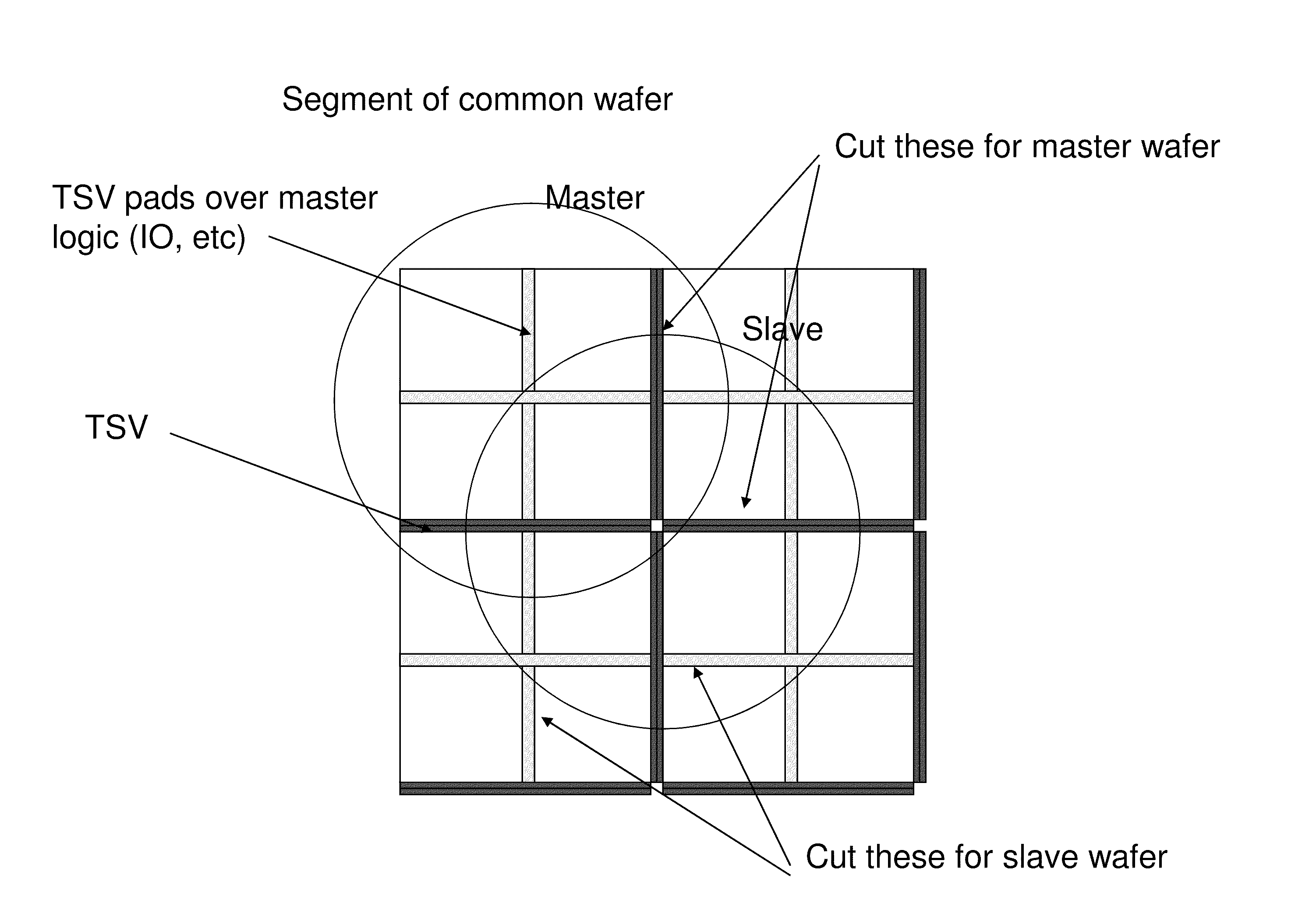
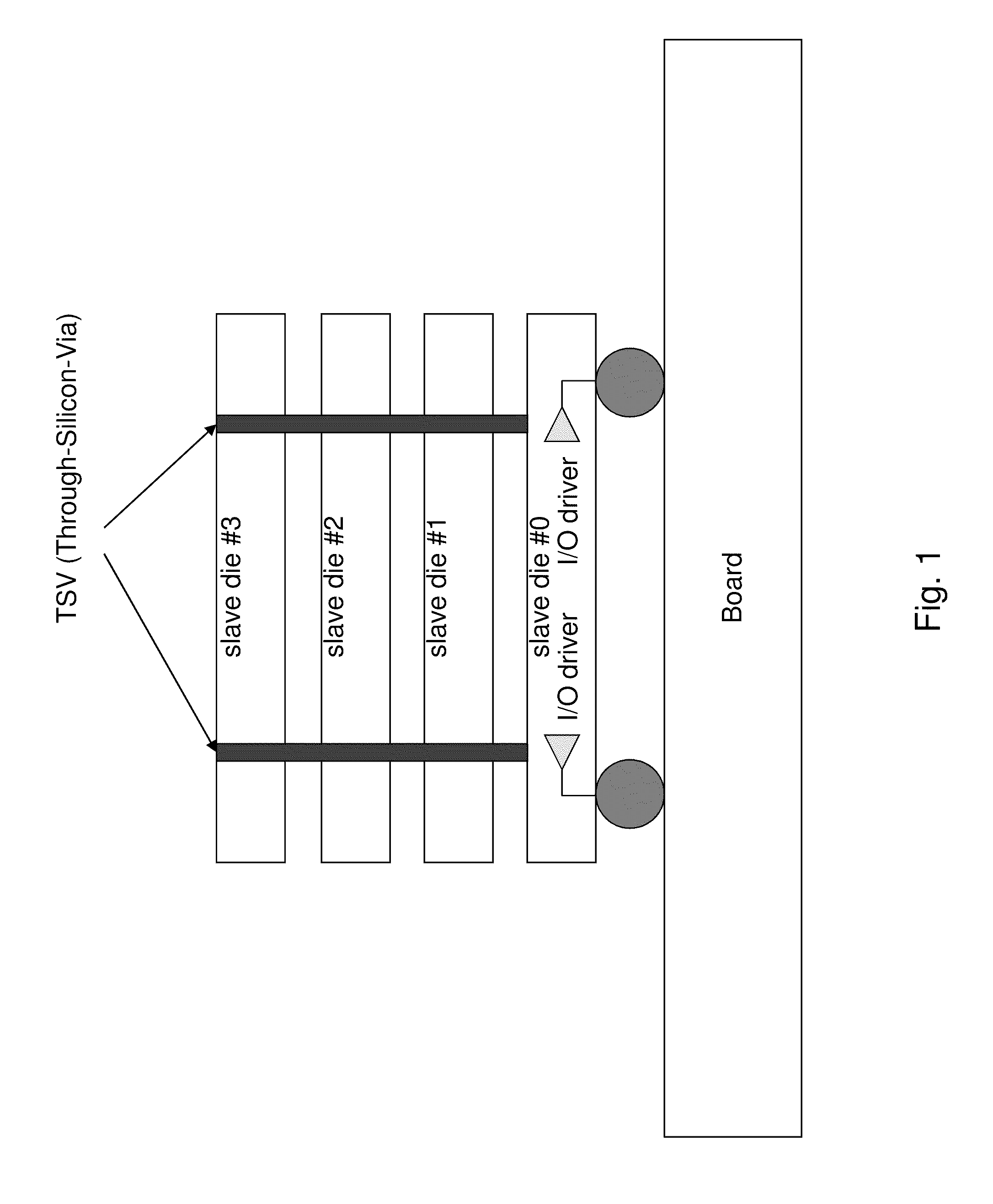
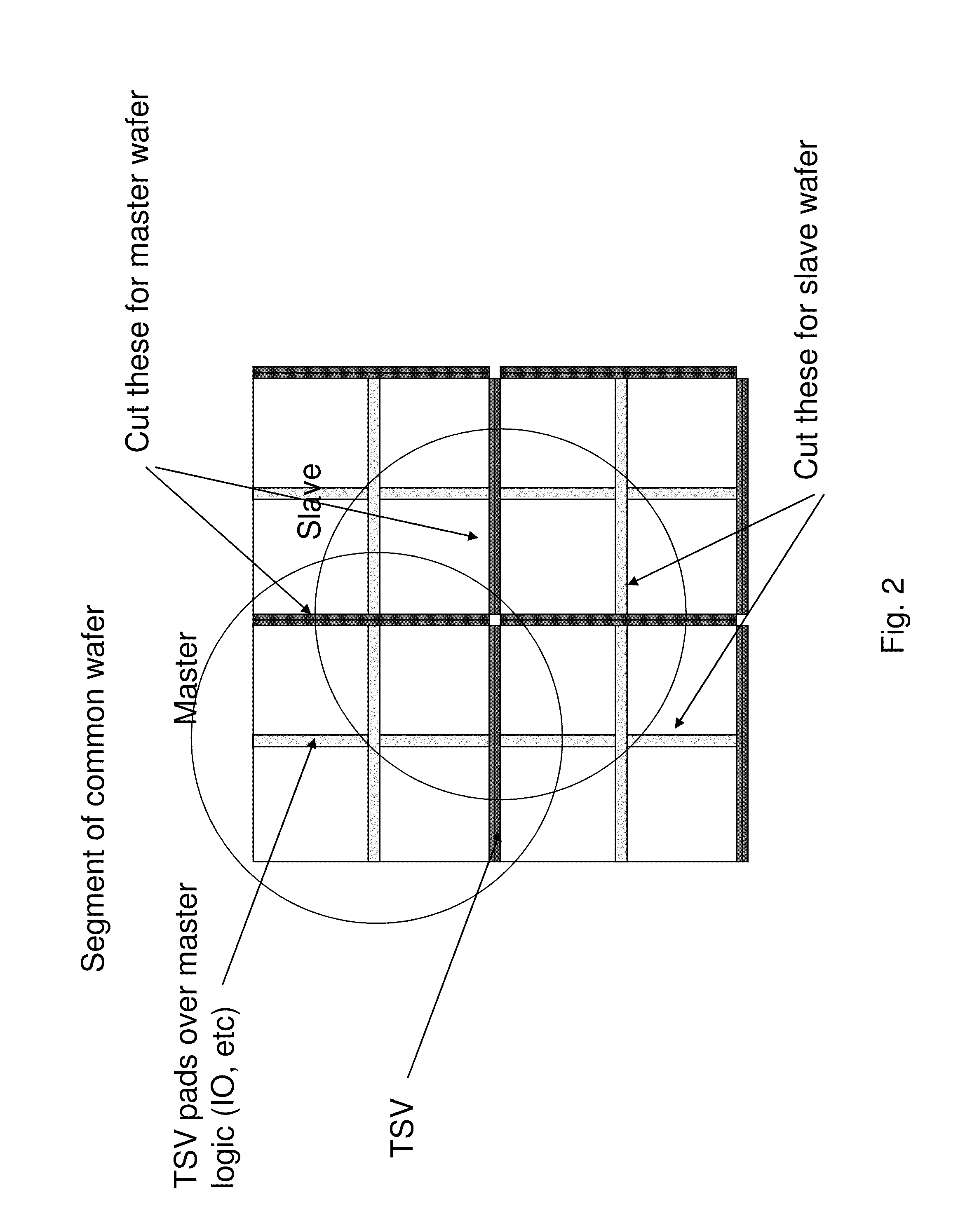
[0020]Turning now to the drawings in greater detail, it will be appreciated that as shown in FIG. 1, a 3D stacked master-slave TSV structure which can be provided where the bottom die interfaces to the outside of the component and upper dies communicate only with the master die using the I / O drivers on master slave die #0 to communicate through the bump connectors to the bump connected board / asic substrate on which the 3D stack structure is mounted. A preferred stack is illustrated in FIG. 7. Just as is shown in FIG. 1, after separation individual circuit dies are stacked as a 3D chip stack bump bonded board / asic substrate carrying said master bus, each die of said 3D chip stack being separated from a single wafer with a common wafer image of integrated circuits which have die ...


PUM


Abstract

A stacked 3D integrated circuit structure is manufactured with a common image design for dies which allows diced master dies to cut from the common wafer and diced slave dies cut to be cut from a wafer which has the common image design. In an embodiment is stacked to form a wafer-to-wafer 3D stack before dicing. Master and slave elements which are used for only one kind of separated individual integrated circuit dies which are located along die edges and at die centers before dicing separation of individual integrated circuit chips. A master wafer is shifted ½ way across a die to make cutting along a kerf line effective to provide both master and slave dies. Multiple slaves can be stacked and coupled to a master die which acts as a bus master when attached to a bus to which only the master die is directly connected. The use of a common wafer design minimizes cost of manufacture of chips destined to be stacked as 3D integrated circuits.

Description

TRADEMARKS[0001]IBM® is a registered trademark of International Business Machines Corporation, Armonk, N.Y., U.S.A. Other names used herein may be registered trademarks, trademarks or product names of International Business Machines Corporation or other companies.BACKGROUND OF THE INVENTION[0002]1. Field of the Invention[0003]This invention relates to a computer processing system, and particularly to integrating different dies formed from a wafer which are used as system elements in stacked master-slave structures.[0004]2. Description of Background[0005]Before our invention U.S. Pat. No. 5,655,113 and its divisional US patents described a computer processing system using a bus system for circuit module architecture system elements to enable a number of memory modules to be coupled in parallel to a master I / O module through a single directional asymmetrical signal swing bus. Semiconductor Equipment and Materials International (SEMI®) a leading organization for standards in the indust...

Claims


Application Information

Patent Timeline
IPC IPC(8): H01L29/06H01L21/00
CPCH01L25/0657H01L25/18H01L25/50H01L2225/06541H01L2225/06513H01L2225/06517H01L2224/16145
Inventor KIM, KYU-HYOUNCOTEUS, PAUL
Owner GLOBALFOUNDRIES INC
Why Eureka
Try Eureka