Multiple die integrated circuit package

a technology of integrated circuits and dies, applied in semiconductor devices, semiconductor/solid-state device details, electrical devices, etc., can solve the problems of increasing manufacturing complexity, inventory control and cost, and the need for a mirror die, and the laminate interposer adds cost and complexity to the finished devi

Active Publication Date: 2009-03-31
SANDISK TECH LLC
View PDF42 Cites 35 Cited by
  • Summary
  • Abstract
  • Description
  • Claims
  • Application Information

AI Technical Summary

Benefits of technology

[0029]In another preferred embodiment, a removable storage card is formed using the packaging apparatus and methods of the invention; an insulator layer is provided with vias formed in selected locations, a first leadframe is positioned overlying the insulator and having some leads overlying the vias in the insulator, a first integrated circuit, which is a nonvolatile memory device, is positioned in proximity to the first leadframe and at least one electrical connection is made between the nonvolatile integrated circuit and the leadframe, a second integrated circuit is provided in proximity to a second leadframe, which is positioned overlying the opposing surface of the insulator and having some leads, which overlie the vias in the insulator, the second integrated circuit being a controller circuit for operating the nonvolatile memory device, the second integrated circuit is electrically connected to the second leadframe.
[0027]In alternative preferred embodiments, the invention may provide an insulator with vias formed in selected locations, a first leadframe overlying one surface of the insulator layer, a second leadframe overlying the opposing insulator layer, a first integrated circuit coupled to the first leadframe using known flip chip technology, where the integrated circuit bond pads are positioned in physical proximity to the desired leads and balls or pads of solder are formed, which are then reflowed using energy to form a mechanical and electrical connection between the die pads and the interior of the leads; the second integrated circuit may likewise be coupled to the second leadframe using flip chip technology, as before the completed device has electrical connections made between the first and second integrated circuits through the vias in the insulator. Since the first and second dies in this preferred embodiment are both coupled to the leadframe using flip chip technology, the integrated circuit devices may be arranged in face-to-face relation.
[0032]In another preferred embodiment, an integrated system may be provided in a single package by incorporating multiple integrated circuit dies on either side of an insulator, the multiple dies being wire bonded to leadframes, which are coupled through vias in the insulator to make arbitrary connections between the integrated circuits, wherein the packaged assembly for the system includes passive elements, such as resistors, capacitors, or inductors. The entire assembly can then be overmolded into a completed packaged system being provided using the methods of the invention.
[0033]Advantages of embodiments of the present invention include providing apparatus and methods of forming multiple integrated circuit modules including multiple integrated circuit devices which are electrically coupled to each other without the need for the complex interposers, flex circuits, laminate substrates or patterned printed circuit boards of the prior art, using conventional wire bonding or flip chip technologies and package molding methods, which are compatible with existing tooling, and using materials compatible with the existing automated semiconductor packaging infrastructure.
[0034]The foregoing description has outlined rather broadly the features and technical advantages of embodiments of the present invention in order that the detailed description of the invention that follows may be better understood. It should be appreciated by those skilled in the art that the conception and specific embodiments disclosed may be readily utilized as a basis for modifying or designing other structures or processes for carrying out the same purposes of the present invention. It should also be realized by those skilled in the art that such equivalent constructions do not depart from the spirit and scope of the invention as set forth in the appended claims.

Problems solved by technology

The need for a “mirror die” greatly increases the complexity of manufacture, inventory control and costs, and requires that each packaged device contain two different dies, having the same function.
Alternatively, an interposer or laminate circuit could be used to enable the back-to-back positioning of two identical functional die, this laminate interposer also adds cost and complexity to the finished device.

Method used


Image

  • Multiple die integrated circuit package
  • Multiple die integrated circuit package
  • Multiple die integrated circuit package

Examples


Embodiment Construction

[0048]The operation and fabrication of the presently preferred embodiments are discussed in detail below. However, the embodiments and examples described are not the only applications or uses contemplated for the invention. The specific embodiments discussed are merely illustrative of specific ways to make and use the invention, and do not limit the scope of the invention. The figures are for illustrative purposes and are not drawn to scale.

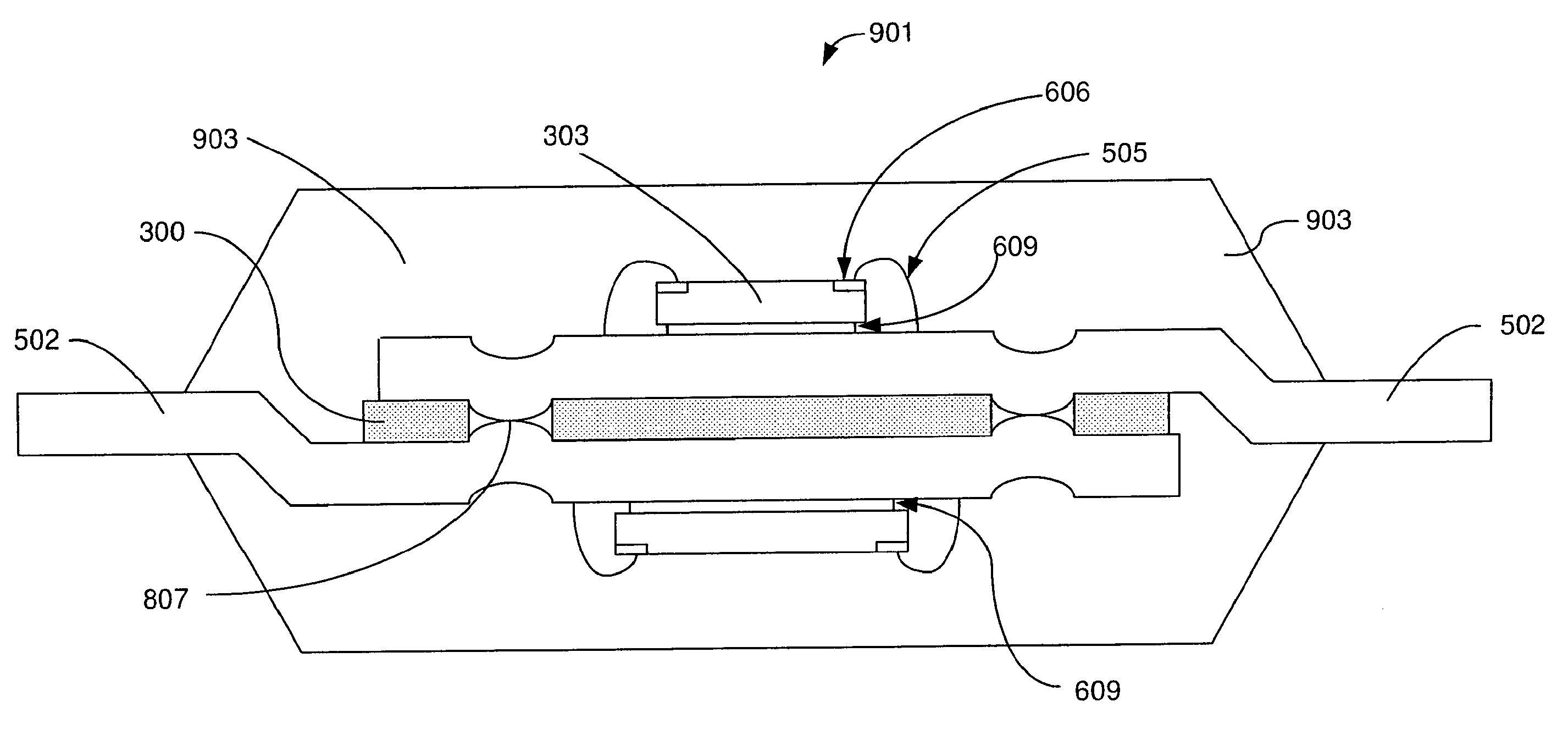
[0049]FIG. 3 depicts a top view of an insulator layer 300 for use in a preferred embodiment of the present invention. The insulator layer 300 may comprise any of many insulating materials, which are compatible with semiconductor processing steps, such as Mylar, Upilex, Kapton, and other films, insulating papers, resins, polyimide, glass, fiberglass, and the like, which are known in the art. Layer 300 is electrically insulating and preferably has physical characteristics compatible with certain thermal processes, such as transfer molding. Through-...


PUM


Abstract

A multiple die package for integrated circuits is disclosed. An insulator layer is provided and one or more vias are formed within it. The insulator may be provided without vias, and vias formed later. At least one integrated circuit is provided and electrically coupled to at least one lead of a first leadframe overlying one surface of the insulator layer. At least one second integrated circuit is provided and electrically coupled to a second leadframe overlying a second surface of the insulator layer. Electrical connections between the two leadframes and the first and second integrated circuits are made through the insulator, at selected locations, by coupling at least one lead of the first and second leadframes one to another. The leads of the first and second leadframe may be physically coupled by a welding process within vias in the insulator. A removable storage card package is also described.

Description

CROSS REFERENCE TO RELATED APPLICATIONS[0001]This application relates to co-pending U.S. patent application Ser. No. 11 / 264,556, entitled “Methods for a Multiple Die Integrated Circuit Package”, filed on even date with this application.TECHNICAL FIELD[0002]The present invention and the various embodiments described generally relate to the fabrication of packaged semiconductor devices including more than one integrated circuit device, and more particularly to fabricating packages with multiple integrated devices to form a packaged system, memory or memory card storage device.BACKGROUND[0003]In the electronics arts, semiconductor devices are provided in packages that protect and provide external connections to the integrated circuits. The need for integration and advanced functionality of the devices has resulted in multiple integrated circuits, sometimes called chips or dies, being provided in a single package. The package can be formed in various ways and of various materials, inclu...

Claims


Application Information

Patent Timeline
Patent Type & Authority Patents(United States)
IPC IPC(8): H01L23/52
CPCH01L23/4951H01L23/49537H01L23/49575H01L24/45H01L25/0657H01L2224/45144H01L2224/48091H01L2224/49171H01L2224/73265H01L2225/06572H01L2924/01046H01L2924/01078H01L2924/01079H01L2924/09701H01L2924/14H01L2924/19041H01L2924/00014H01L24/48H01L24/49H01L2924/01087H01L2224/32225H01L2224/32245H01L2224/48227H01L2224/48247H01L2924/00H01L2924/01013H01L2924/01028H01L2924/00012H01L2224/32014H01L2224/49113H01L24/73H01L2924/181H01L2224/05554
Inventor WALLACE, BOB
Owner SANDISK TECH LLC
Why Eureka
Try Eureka