Thin film transistor and its preparation method, array substrate, display device

A technology of thin film transistor and transition layer, applied in transistor, semiconductor/solid-state device manufacturing, semiconductor device and other directions, can solve the problems of large contact resistance and complex process, reduce the probability of short circuit, increase the on-state current, and reduce the signal delayed effect

Active Publication Date: 2022-04-15
BOE TECH GRP CO LTD
View PDF3 Cites 0 Cited by
  • Summary
  • Abstract
  • Description
  • Claims
  • Application Information

AI Technical Summary

Problems solved by technology

However, for the TFT in this technical solution, due to the large contact resistance between the active layer and the source-drain electrodes, the process of conducting the active layer is required, which makes the process of preparing this TFT complicated.

Method used


Image

  • Thin film transistor and its preparation method, array substrate, display device
  • Thin film transistor and its preparation method, array substrate, display device
  • Thin film transistor and its preparation method, array substrate, display device

Examples


Embodiment Construction

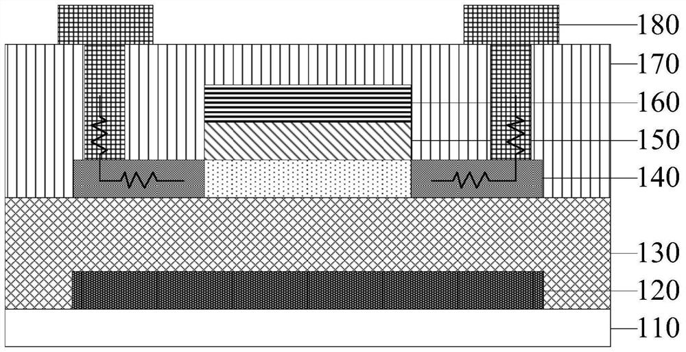
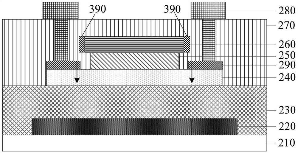
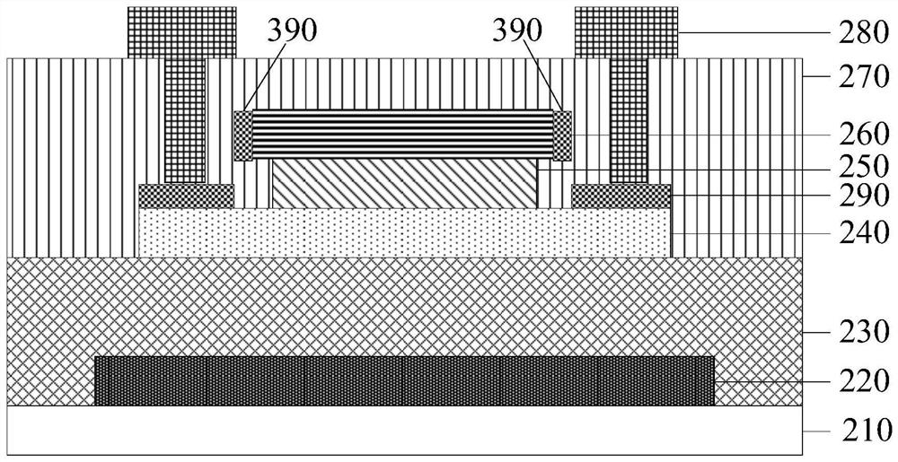
[0027] Example embodiments will now be described more fully with reference to the accompanying drawings. Example embodiments may, however, be embodied in many forms and should not be construed as limited to the examples set forth herein; rather, these embodiments are provided so that this disclosure will be thorough and complete, and will fully convey the concept of example embodiments to those skilled in the art. The described features, structures, or characteristics may be combined in any suitable manner in one or more embodiments. In the following description, numerous specific details are provided in order to give a thorough understanding of embodiments of the present disclosure. However, those skilled in the art will appreciate that the technical solutions of the present disclosure may be practiced without one or more of the specific details being omitted, or other methods, components, devices, steps, etc. may be adopted. In other instances, well-known technical solutio...


PUM


Abstract

The disclosure relates to a thin film transistor, a preparation method thereof, an array substrate, and a display device, and belongs to the field of display technology. The thin film transistor includes: a substrate; an active layer disposed on the substrate; a gate insulating layer disposed on the active layer; a gate layer disposed on the gate insulating layer; an interlayer an insulating layer, disposed on the substrate, the active layer, and the gate layer; a source-drain metal layer, disposed on the interlayer insulating layer; a first transition layer, disposed on the active layer Between the source and drain metal layer; the second transition layer is arranged on the side of the gate layer. The technical solution of the present disclosure can reduce parasitic resistance and signal delay.

Description

technical field [0001] The present disclosure relates to the field of display technology, in particular, to a thin film transistor and a manufacturing method thereof, an array substrate, and a display device. Background technique [0002] Compared with traditional silicon-based thin-film transistors (Si-TFTs), metal oxide thin-film transistors represented by IGZO TFT (Thin Film Transistor, thin-film transistor) are famous for their high mobility, good uniformity, and simple manufacturing process. get rapid development. [0003] In the technical solution of OLED (Organic Light-Emitting Diode, Organic Light-Emitting Diode) display with relatively high resolution, thin film transistors with a top-gate self-aligned structure are generally used. However, for the TFT in this technical solution, due to the large contact resistance between the active layer and the source-drain electrodes, a process of conducting the active layer is required, which complicates the process of prepari...

Claims


Application Information

Patent Timeline
Patent Type & Authority Patents(China)
IPC IPC(8): H01L29/786H01L21/34
CPCH01L29/66969H01L29/78606H01L29/78618H01L29/7869
Inventor 王国英宋振
Owner BOE TECH GRP CO LTD
Why Eureka
Try Eureka