Novel slice type semiconductor ultra-thin packaging device

A packaging device and semiconductor technology, which is applied in semiconductor/solid-state device manufacturing, electrical components, circuits, etc., can solve problems such as difficult placement and troublesome installation, and achieve the effect of ensuring accuracy

Active Publication Date: 2018-09-14
广东协铖微电子科技有限公司
View PDF2 Cites 7 Cited by
  • Summary
  • Abstract
  • Description
  • Claims
  • Application Information

AI Technical Summary

Problems solved by technology

[0002] At present, with the advancement of science and technology, people are increasingly pursuing low-cost, high-efficiency small-volume packaging in the production of chips in the electronics industry. As a very suitable packaging material, resin film has gradually entered people's field of vision. Compared with traditional The plastic sealing film used in the process, the resin film can also be packaged in an ultra-thin state, which greatly reduces the occupied space, but the ultra-thin volume also makes the installation troublesome and difficult for workers to install in the process of gluing and pressing. question

Method used


Image

  • Novel slice type semiconductor ultra-thin packaging device
  • Novel slice type semiconductor ultra-thin packaging device
  • Novel slice type semiconductor ultra-thin packaging device

Examples


Embodiment Construction

[0015] The following will clearly and completely describe the technical solutions in the embodiments of the present invention with reference to the accompanying drawings in the embodiments of the present invention. Obviously, the described embodiments are only some, not all, embodiments of the present invention. Based on the embodiments of the present invention, all other embodiments obtained by persons of ordinary skill in the art without making creative efforts belong to the protection scope of the present invention.

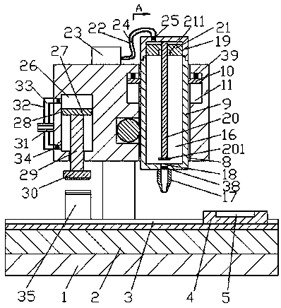
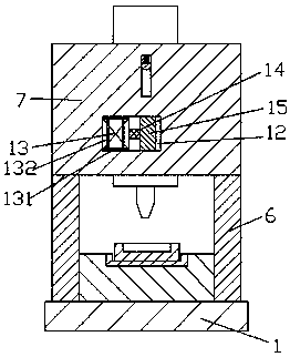
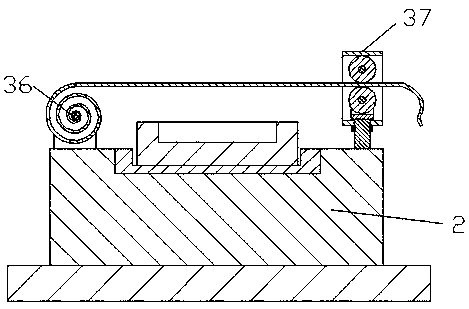
[0016] see Figure 1-6, an embodiment provided by the present invention: a new chip semiconductor ultra-thin packaging device, including a fixed base 1, a conveying line 2 extending left and right is arranged at the middle position of the upper end surface of the fixed base 1, and the A fixed conveying channel 3 is provided at the middle position of the upper end surface of the conveying assembly line 2, and a conveying trolley 4 is housed in the fixed conveyi...


PUM


Abstract

The invention discloses a novel slice type semiconductor ultra-thin packaging device comprising a fixed base. A conveying assembly line extending left and right is arranged in the middle of the upperend surface of the fixed base. Sealing space is formed in the left side inside a fixed case; a hydraulic rod is fixedly connected to the central position of the lower end surface of a sealing plate; the lower end of the hydraulic rod passes through the lower end wall of the sealing space and is fixedly connected with a press-fit plate; a resin conveying device is arranged right below the press-fitplate and includes a winding mechanism and a pulling mechanism. When the packaging device is working, an extruding plate moves up and down along a guiding rod without falling based on cooperation ofan annular clamp plate and an annular clamp slot; the extruding plate can fall to be in contact with the lower end wall of glue storage space to prevent plugging of a glue coating needle due to solidification of lower-end glue liquid not in use for long time; and the resin sheet that is not used can be switched automatically, so that precision is improved and the work efficiency is enhanced.

Description

technical field [0001] The invention relates to the field of semiconductor packaging, in particular to a novel chip-type semiconductor ultra-thin packaging device. Background technique [0002] At present, with the advancement of science and technology, people are increasingly pursuing low-cost, high-efficiency small-volume packaging in the production of chips in the electronics industry. As a very suitable packaging material, resin film has gradually entered people's field of vision. Compared with traditional The plastic sealing film used in the process, the resin film can also be packaged in an ultra-thin state, which greatly reduces the occupied space, but the ultra-thin volume also makes the installation troublesome and difficult for workers to install in the process of gluing and pressing. question. Contents of the invention [0003] The object of the present invention is to provide a novel chip-type semiconductor ultra-thin packaging device to solve the problems rai...

Claims


Application Information

Patent Timeline
Patent Type & Authority Applications(China)
IPC IPC(8): H01L21/67H01L21/687H01L21/50
CPCH01L21/50H01L21/67126H01L21/687
Inventor 岑森参
Owner 广东协铖微电子科技有限公司
Why Eureka
Try Eureka