A planar metal nano-chiral structure, preparation method and at effect regulation method
A metal nanostructure and metal nanotechnology, applied in nonlinear optics, instruments, optics, etc., can solve the problems of complex structure, low preparation efficiency, weak signal of single-layer structure, etc., and achieve the effect of enhancing asymmetric transmission signals.
- Summary
- Abstract
- Description
- Claims
- Application Information
AI Technical Summary
Problems solved by technology
Method used
Image

Examples
Embodiment 1
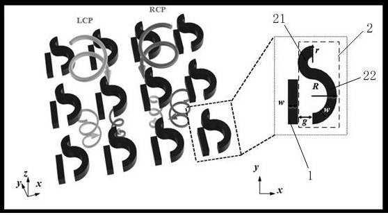
[0047] Such as figure 1 As shown, in order to solve the existing technical problems of realizing the asymmetric transmission effect of circularly polarized light, such as complex structure, weak effect, and low preparation efficiency, this embodiment provides a planar metal nano-chiral structure that realizes high-efficiency direct-incident asymmetric transmission , a chiral structure composed of a plurality of nano-units with the same structure up-down and left-right; the metal nano-unit includes a metal nanorod 1 and a coplanar S-shaped metal nanostructure 2 next to the metal nanorod 1 . S-shaped metal nanostructures are designed with chiral features. The metal nanorod 1 is a cuboid, and the S-shaped metal nanostructure 2 is an integrated structure formed by connecting the first arc structure 21 and the second arc structure 22 end to end. The first arc structure 21 and the second arc structure 22 are The diameters are different, and the opening direction is opposite, the di...
Embodiment 2
[0069] The invention also includes a method for regulating the AT effect of the planar metal nano-chiral structure. This example is based on the parameters and steps of Example 1. After preparing the planar metal nanochiral structure of the present invention to achieve high-efficiency direct-incident asymmetric transmission, the following structural parameter changes are performed to regulate the AT signal and spectrum.
[0070] Such as Image 6 As shown, the parameter to set the structure of the metal nanorod width w = 40nm with a thickness of 50 nm; the width of the S-shaped metal nanostructure w = 40nm, and the thickness is 50 nm; the outer diameters of the two semicircular rings of the S-shaped metal nanostructure are r =60 nm and R = 100 nm; the metal nanorod 1 The spacing in the x-direction from the tail end of the S-shaped metal nanostructure 2 is defined as g =60nm; the central angles of the first arcuate structure 21 and the second arcuate structure 22 are bo...
Embodiment 3
[0074] The difference from the above-mentioned embodiment 2 is that this embodiment only changes the distance between the metal nanorods and the S-shaped metal nanostructures g The value of , other parameters take fixed values within the range of each parameter: the width of metal nanorods w = 40nm, length l = 160 nm with a thickness of 50 nm; the width of the S-shaped metal nanostructure w = 40nm, and the thickness is 50 nm; the outer diameters of the two semicircular rings of the S-shaped metal nanostructure are r = 60 nm and R = 100 nm; the central angles of the first arc-body structure 21 and the second arc-body structure 22 are both 180°. Transforming the distance between the metal nanorods and the tail end of the S of the S-shaped metal nanostructure 2 in the x direction is defined as g parameter range, g The values are respectively 20 nm, 40 nm, 60 nm, 80 nm, and 100 nm. When preparing the structure of this embodiment, use a pattern generator to set the str...
PUM
| Property | Measurement | Unit |
|---|---|---|
| width | aaaaa | aaaaa |
| thickness | aaaaa | aaaaa |
| length | aaaaa | aaaaa |
Abstract
Description
Claims
Application Information
 - R&D
- Intellectual Property
- Life Sciences
- Materials
- Tech Scout
- Unparalleled Data Quality
- Higher Quality Content
- 60% Fewer Hallucinations
Browse by: Latest US Patents, China's latest patents, Technical Efficacy Thesaurus, Application Domain, Technology Topic, Popular Technical Reports.
© 2025 PatSnap. All rights reserved.Legal|Privacy policy|Modern Slavery Act Transparency Statement|Sitemap|About US| Contact US: help@patsnap.com