Bonding impedance detecting system and method

A technology of impedance detection and bonding, which is applied in the direction of measuring resistance/reactance/impedance, measuring devices, measuring electrical variables, etc., can solve the problems of large influence on display effect, inability to bond and automatically detect impedance uniformity, etc., and achieve the goal of reducing the impact Effect

Active Publication Date: 2018-09-28
BOE TECH GRP CO LTD +1
View PDF9 Cites 5 Cited by
  • Summary
  • Abstract
  • Description
  • Claims
  • Application Information

AI Technical Summary

Problems solved by technology

It is impossible to automatically detect the bonding impedance and its uniformity, so that the abnormal bonding impedance has a greater impact on the display effect

Method used


Image

  • Bonding impedance detecting system and method
  • Bonding impedance detecting system and method
  • Bonding impedance detecting system and method

Examples


Embodiment Construction

[0035] In order to enable those skilled in the art to better understand the technical solution of the present invention, the technical solution in the present invention will be clearly and completely described below in conjunction with the accompanying drawings. Obviously, the described embodiments are part of the embodiments of the present invention, and Not all examples. Based on the embodiments of the present invention, all other embodiments obtained by persons of ordinary skill in the art without making creative efforts belong to the protection scope of the present invention.

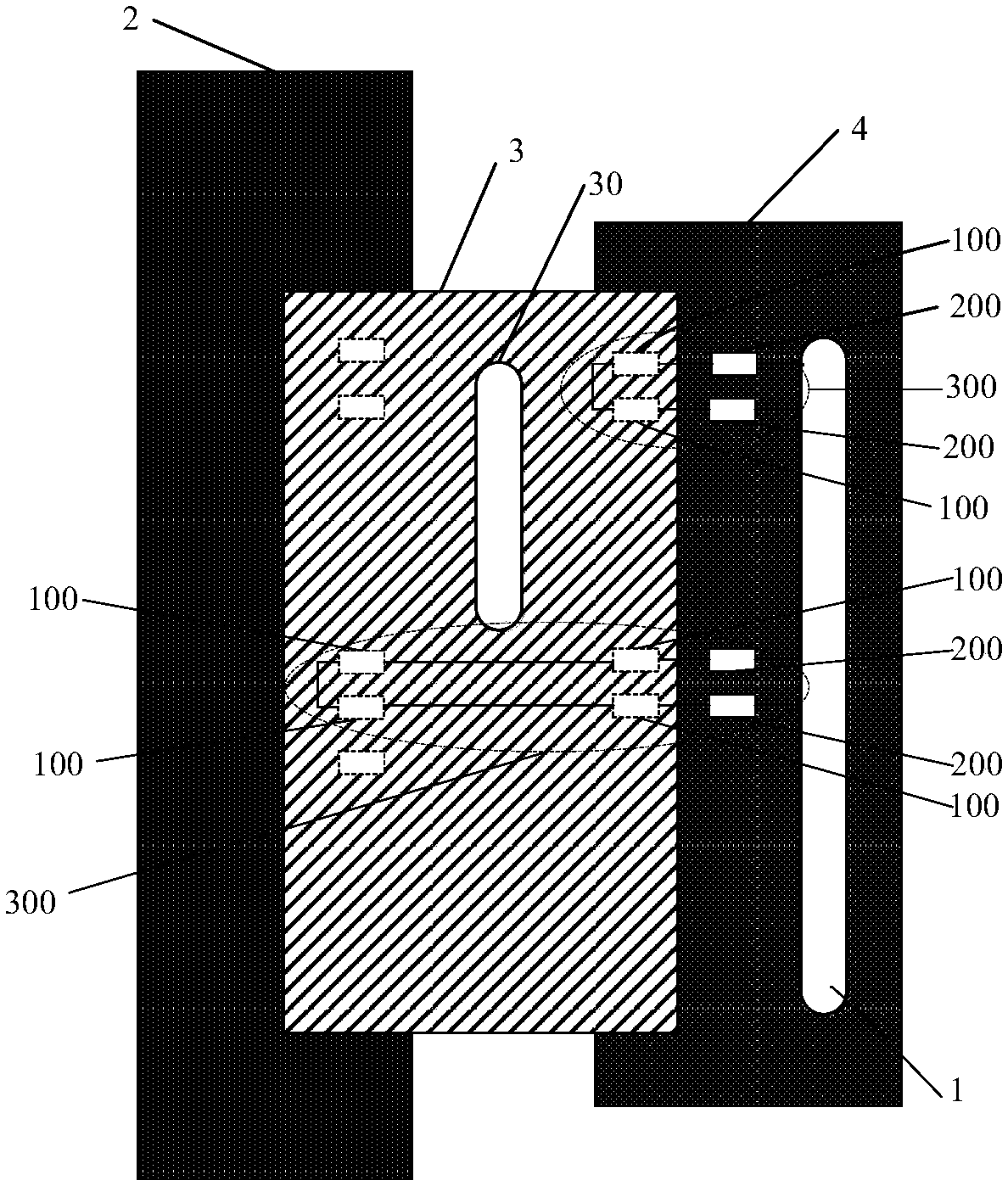
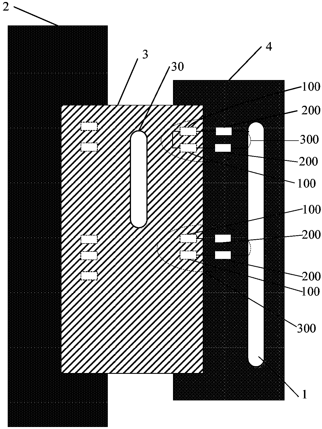
[0036] figure 1 It is a schematic structural diagram of a bonding impedance detection system provided in Embodiment 1 of the present invention, as shown in figure 1 As shown, the bonding impedance detection system includes a bonding impedance detection module 1, a display panel 2, a chip-on-chip film 3 and a circuit board 4, and the chip-on-chip film 3 and the circuit board 4 pass through a plurali...


PUM


Abstract

The invention discloses a bonding impedance detecting system and method. The bonding impedance detecting system comprises a bonding impedance detecting module, a display panel, a chip-on-film and a circuit board, wherein the chip-on-film is connected with the circuit board through a plurality of bonding pad groups; the chip-on-film is connected with the display panel through a plurality of bondingpad groups; each bonding pad group comprises two bonding pads which are connected; part of the bonding pad groups and a first equivalent resistor connected with the part of the bonding pad groups form a detecting structure; the detecting structure is connected with a bonding impedance detecting module; and the bonding impedance detecting module is used for detecting the bonding impedance of the bonding pad groups and the uniformity of the bonding impedance of the bonding pad groups. The bonding impedance of a display screen and the uniformity of the bonding impedance can be detected, and influences of bonding impedance abnormity to the display effect of the display screen are reduced effectively.

Description

technical field [0001] The invention relates to the field of display panels, in particular to a bonding impedance detection system and method. Background technique [0002] In the production process of the display screen, such as OLED (Organic Light-Emitting Diode, organic light-emitting diode) display production process, FPC (Flexible Printed Circuit, flexible circuit board) and COF (Chip OnFlex, or, Chip On Film, Chip-on-chip film) and the connection between COF and display panel are all realized by bonding process. Specifically, the bonding process uses ACF glue (Anisotropic Conductive Film, anisotropic conductive film) to connect FPC and COF and COF and display panel. Connect together through corresponding PAD (pad in printed circuit board). The number of particles of the ACF glue, the temperature and time of the bonding connection, the material of the ACF glue, and the cleanliness of the PAD will all cause changes in the bonding impedance. [0003] With the accelerati...

Claims


Application Information

Patent Timeline
Patent Type & Authority Applications(China)
IPC IPC(8): G01R27/02
CPCG01R27/02
Inventor 张斌陈鹏名许文鹏
Owner BOE TECH GRP CO LTD
Why Eureka
Try Eureka