Plasma etching machine for semiconductor chip

A plasma and etching machine technology, which is applied in semiconductor/solid-state device manufacturing, electrical components, circuits, etc., can solve problems affecting reaction efficiency, hindrance, and wafer processing quality, and achieve improved cleaning effect and large compression Effect

Active Publication Date: 2020-10-13
广东汉岂工业技术研发有限公司
View PDF5 Cites 1 Cited by
  • Summary
  • Abstract
  • Description
  • Claims
  • Application Information

AI Technical Summary

Problems solved by technology

This solution achieves sustainable etching regardless of the volatility of the etching reaction product, but the reaction product generated on the wafer etching reaction surface cannot be eliminated in time, which hinders the progress of new reactions, thereby affecting the reaction efficiency; If the reaction gas injection is too concentrated, the ionized ions will bombard the local area of ​​the wafer too concentratedly, resulting in uneven etching of the reaction surface and affecting the quality of wafer processing

Method used


Image

  • Plasma etching machine for semiconductor chip
  • Plasma etching machine for semiconductor chip
  • Plasma etching machine for semiconductor chip

Examples


Embodiment Construction

[0025] In order to make the technical means, creative features, goals and effects achieved by the present invention easy to understand, the present invention will be further described below in conjunction with specific embodiments.

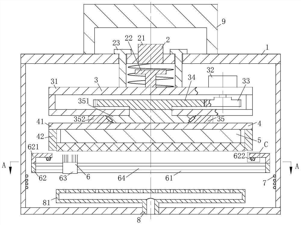
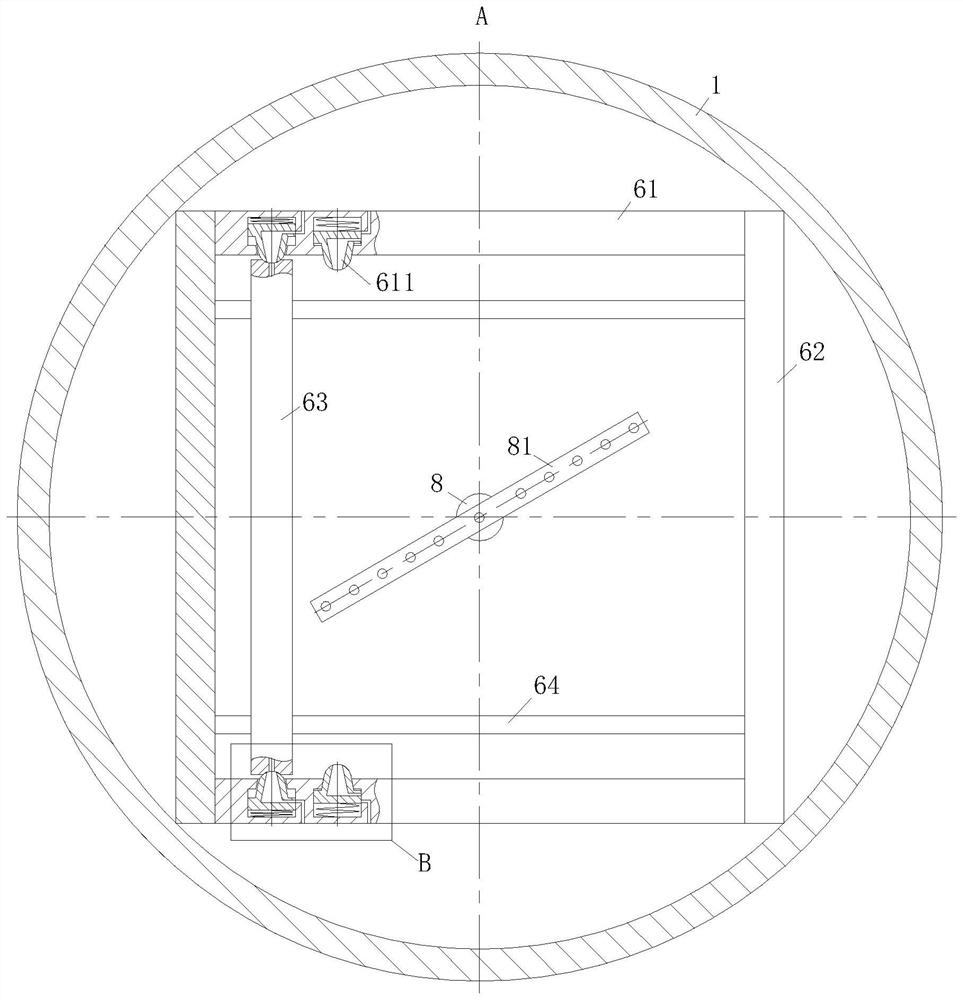
[0026] Such as Figure 1 to Figure 6 As shown, a semiconductor chip plasma etching machine according to the present invention includes a box body 1, a vibrating device 2, a rotating device 3, a clamping device 4, a heater 5, a suction device 6, an excitation coil 7, and an air supply device 8. Bias supply device 9, a bias supply device 9 is provided above the top plate of the box body 1; the bias voltage supply device 9 is used to apply a bias voltage to the wafer; a vibration device is provided below the top plate of the box body 1 2; the vibrating device 2 is used to vibrate the wafer; a rotating device 3 is provided below the vibrating device 2, and the rotating device 3 is used to provide power for the wafer to rotate; a clamp is provided belo...


PUM


Abstract

The invention belongs to the technical field of semiconductor chip manufacturing and in particular relates to a semiconductor chip plasma etching machine which comprises a box body, a vibration device, a rotating device, a clamping device, a heating device, a suction device, an excitation wire coil, a gas supply device and a bias voltage providing device, wherein the bias voltage providing deviceis used for applying bias voltage to a wafer, the vibration device is used for vibrating the wafer, the rotating device is used for rotating the wafer via the clamping device, the suction device is used for removing reaction products on a wafer reaction surface, the excitation wire coil is used for ionizing a reaction gas, and the gas supply device is for conveying the reaction gas and then uniformly spraying the reaction gas; via arrangement of the rotating device, the reaction surface of the wafer is enabled to receive uniform bombardment of ions, and therefore processing quality of the wafer can be further improved; via arrangement of a removal plate, the reaction products generated by the reaction surface of the wafer can be removed, and therefore the reaction efficiency can be improved.

Description

technical field [0001] The invention belongs to the technical field of semiconductor chip manufacturing, in particular to a semiconductor chip plasma etching machine. Background technique [0002] Wafer refers to the silicon chip used in the production of silicon semiconductor integrated circuits. Wafer is the carrier used in the production of integrated circuits. In general, wafers refer to single crystal silicon wafers. Wafer is the most commonly used semiconductor material. According to its diameter, it is divided into 4 inches, 5 inches, 6 inches, 8 inches and other specifications. Recently, 12 inches or even larger specifications have been developed. The larger the wafer, the more ICs that can be produced on the same wafer, which can reduce costs; but the requirements for material technology and production technology are higher, such as uniformity and so on. It is generally believed that the larger the diameter of the silicon wafer, it means that the fab has better tec...

Claims


Application Information

Patent Timeline
Patent Type & Authority Patents(China)
IPC IPC(8): H01L21/67
CPCH01L21/67011H01L21/67017H01L21/67069
Inventor 陈涛何蓉
Owner 广东汉岂工业技术研发有限公司
Why Eureka
Try Eureka