Production method of fine circuit of single-sided COF flexible substrate and product obtained through production method
A flexible substrate and fine circuit technology, which is applied in the production of COF single-sided flexible substrate fine circuit and its products, can solve the problem that the minimum line width/line spacing does not reach 10 microns, etc.
- Summary
- Abstract
- Description
- Claims
- Application Information
AI Technical Summary
Problems solved by technology
Method used
Image
Examples
Embodiment 1
[0028] The fine circuit of COF single-sided flexible substrate is made by the following steps:
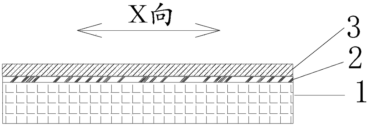
[0029] (1) Dry film lamination: a metal Ni / Cr layer 2 with a thickness of 20 nanometers is set on the upper surface of the polyimide lower layer 1, and a copper layer 3 with a thickness of 1 micron is set on the upper surface of the metal Ni / Cr layer 2 Make the substrate, and form a dry film with a thickness of 15 microns by vacuum pressing on the upper surface of the copper layer 3;
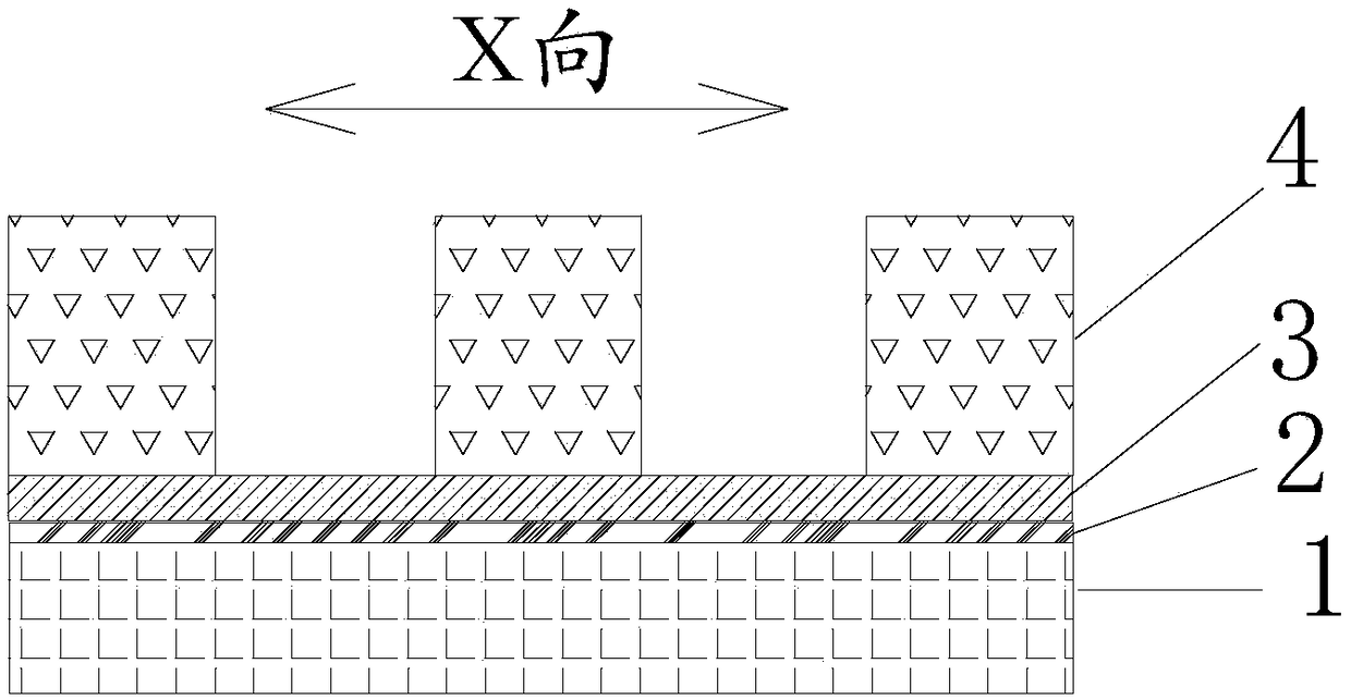
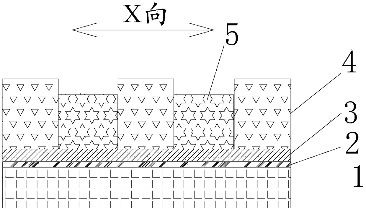
[0030] (2) UV exposure of dry film: cover the glass negative on the dry film, the glass negative includes transparent areas and black areas spaced one by one in the X direction, the size of each transparent area in the X direction is 5 microns, each black The X-direction size of the area is 9 microns. Use ultraviolet rays to irradiate and expose the dry film covered with the glass negative film and then remove the glass negative film. The part covered by the transparent area on the dry film is the ex...
Embodiment 2
[0038] The difference from Example 1 is: in step (2), the X-direction dimension of each transparent area and dry film exposed portion 4 is 4 microns, and the X-direction dimension of each black area and dry film unexposed portion is 10 microns. Micron.
Embodiment 3
[0040] The difference from Example 1 is: in step (1), the thickness of copper layer 3 is 0.5 micron; in step (2), the X-direction size of each transparent area and dry film exposure part 4 is 6 microns, each Both the black area and the unexposed portion of the dry film had an x-dimension of 8 microns.
PUM
| Property | Measurement | Unit |
|---|---|---|
| thickness | aaaaa | aaaaa |
| size | aaaaa | aaaaa |
| thickness | aaaaa | aaaaa |
Abstract
Description
Claims
Application Information


