A method for manufacturing a COF double-sided flexible substrate fine circuit and a product thereof
A technology of fine lines and fabrication methods, applied in the exposure method of radiation-sensitive masks, the manufacture of printed circuits, the removal of conductive materials by chemical/electrolytic methods, etc. question
- Summary
- Abstract
- Description
- Claims
- Application Information
AI Technical Summary
Problems solved by technology
Method used
Image
Examples
Embodiment 1
[0031] The fine circuit of COF double-sided flexible substrate is made by the following steps:
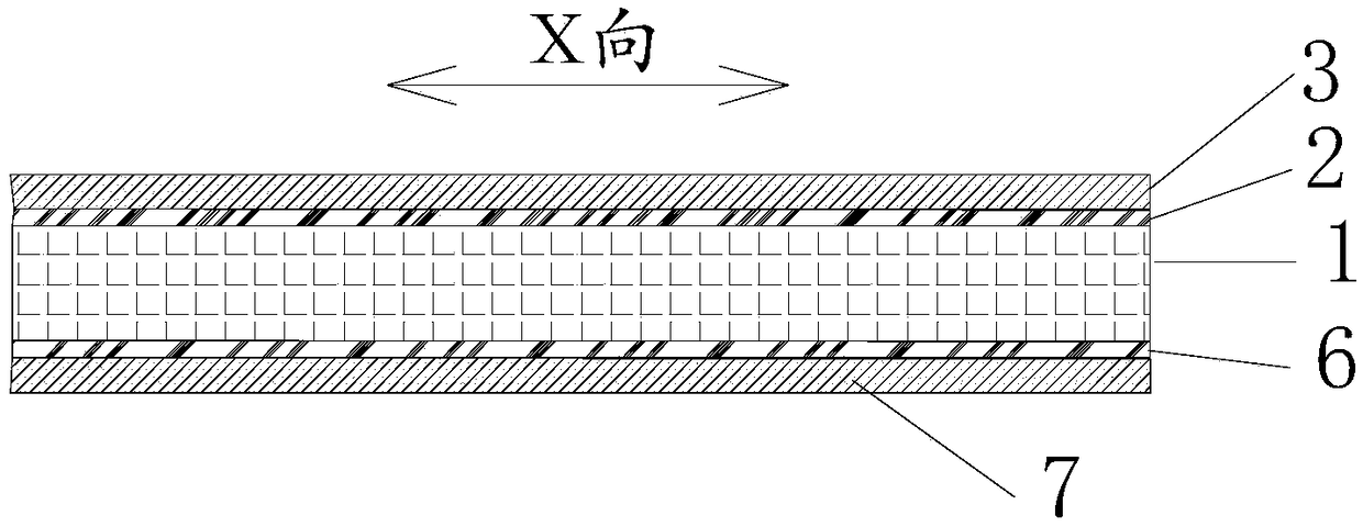
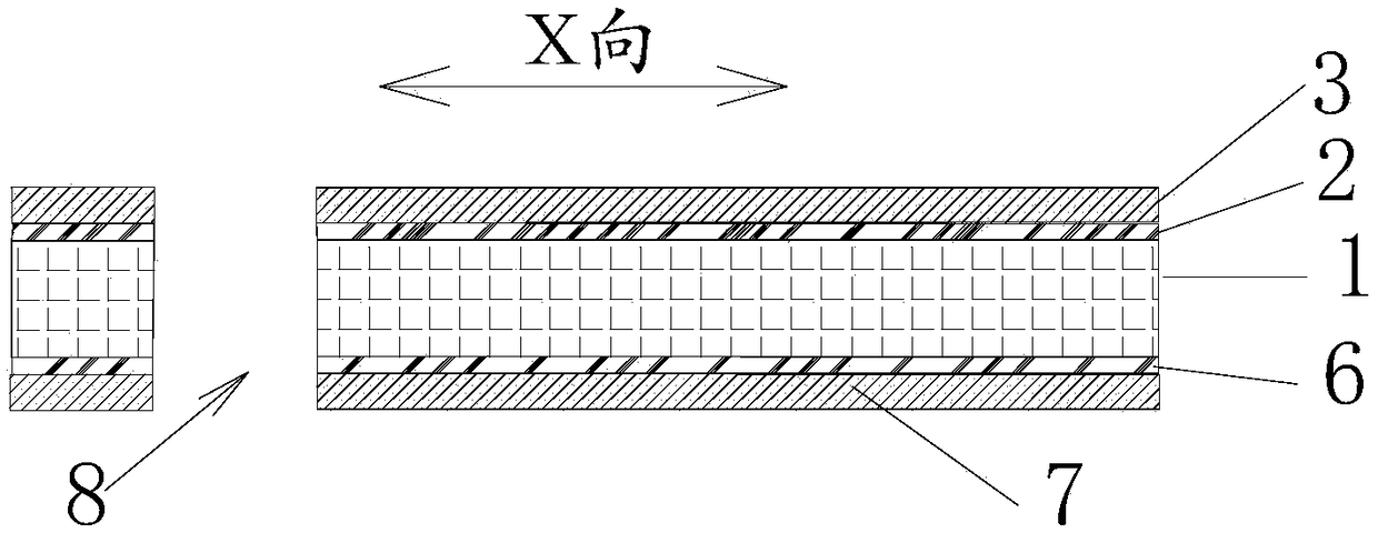
[0032] (1) Laser drilling: the upper metal Ni / Cr layer 2 is set on the upper surface of the polyimide interlayer 1, the lower metal Ni / Cr layer 6 is set on the lower surface of the polyimide interlayer 1, and the upper metal The upper surface of the Ni / Cr layer 2 is provided with an upper copper layer 3, and the lower surface of the lower metal Ni / Cr layer 6 is provided with a lower copper layer 7 to make a base material, and a through hole 8 penetrating the entire base material is lasered on the base material. The thickness of the metal Ni / Cr layer and the lower metal Ni / Cr layer is 20 nanometers, and the thickness of the upper copper layer 3 and the lower copper layer 7 is 1 micron;
[0033] (2) In-hole metallization: deposit a conductive film layer on the inner wall of the through hole 8;
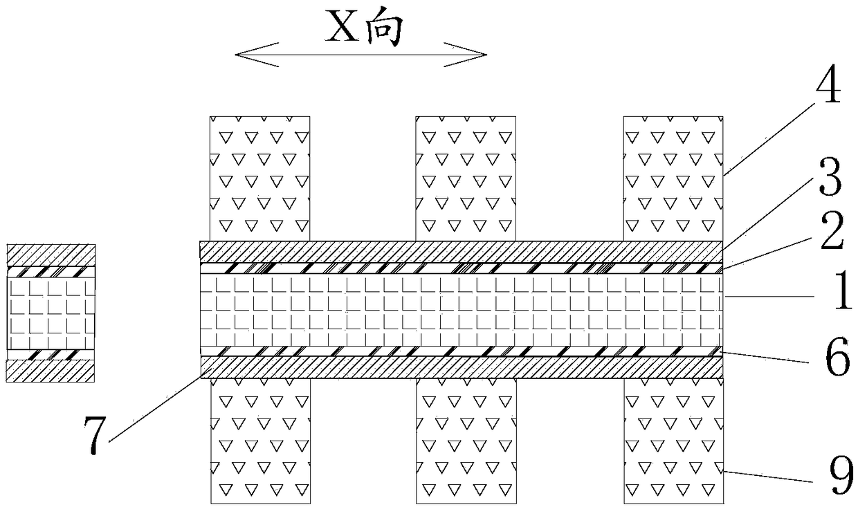
[0034] (3) Dry film lamination: form the upper dry film by lamination on the upper surfa...
Embodiment 2
[0043] The difference from Example 1 is: in step (4), the X-direction size of each upper and lower transparent area and the upper and lower dry film exposure part 4 is 4 microns, each upper and lower black area and the upper and lower The X-direction dimension of the unexposed part of the dry film is 10 microns.
Embodiment 3
[0045] The difference from Example 1 is: in step (1), the thickness of the upper and lower copper layers 3 is 0.5 micron; The dimensions in the X direction of each of the upper and lower black areas and the unexposed parts of the upper and lower dry films are all 8 microns in the X direction.
PUM
| Property | Measurement | Unit |
|---|---|---|
| thickness | aaaaa | aaaaa |
| thickness | aaaaa | aaaaa |
| size | aaaaa | aaaaa |
Abstract
Description
Claims
Application Information


