A kind of manufacturing method and product of cof double-sided flexible substrate fine circuit

A manufacturing method, a technology of fine lines, applied in the exposure method of radiation-sensitive masks, the manufacture of printed circuits, the removal of conductive materials by chemical/electrolytic methods, etc., which can solve the problem that the minimum line width/line spacing does not reach 10 microns question

Active Publication Date: 2020-02-07
MFLEX YANCHENG CO LTD
View PDF4 Cites 0 Cited by
  • Summary
  • Abstract
  • Description
  • Claims
  • Application Information

AI Technical Summary

Problems solved by technology

At present, most of the companies that have mastered the production technology of COF flexible substrates and have the conditions for mass production are concentrated in South Korea, Japan, and Taiwan, China. Individual companies in mainland China have the production capacity to use etching methods to produce single-sided COF flexible substrates, but the minimum line width / line The distance does not reach the level of 10 microns / about 10 microns

Method used


Image

  • A kind of manufacturing method and product of cof double-sided flexible substrate fine circuit
  • A kind of manufacturing method and product of cof double-sided flexible substrate fine circuit
  • A kind of manufacturing method and product of cof double-sided flexible substrate fine circuit

Examples


Embodiment 1

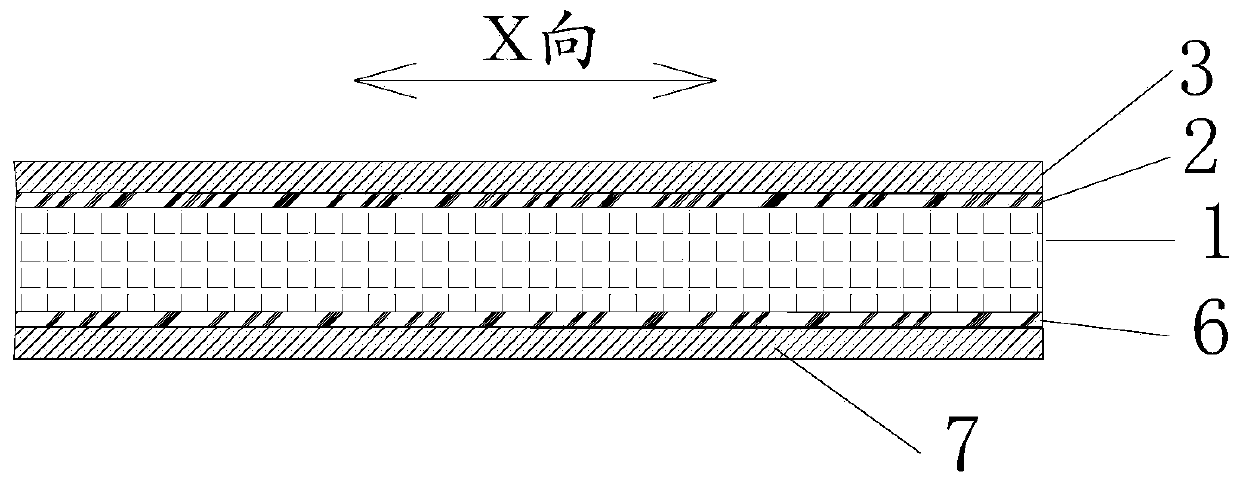
[0031] The fine circuit of COF double-sided flexible substrate is made by the following steps:

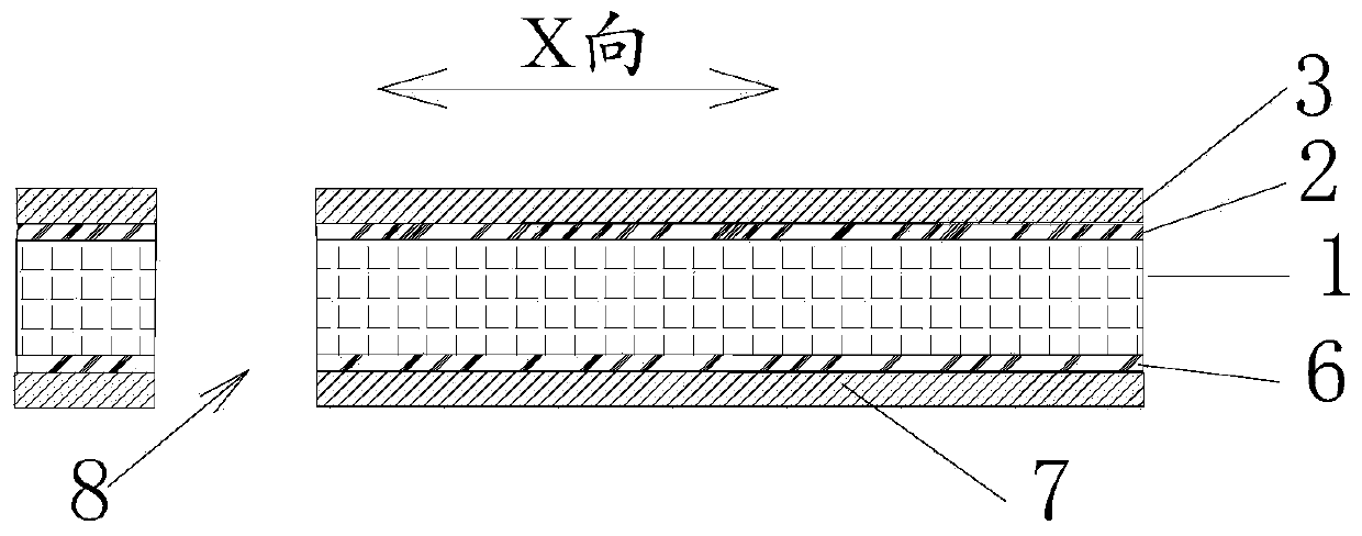
[0032] (1) Laser drilling: the upper metal Ni / Cr layer 2 is set on the upper surface of the polyimide interlayer 1, the lower metal Ni / Cr layer 6 is set on the lower surface of the polyimide interlayer 1, and the upper metal The upper surface of the Ni / Cr layer 2 is provided with an upper copper layer 3, and the lower surface of the lower metal Ni / Cr layer 6 is provided with a lower copper layer 7 to make a base material, and a through hole 8 through the entire base material is lasered on the base material. The thickness of the metal Ni / Cr layer and the lower metal Ni / Cr layer is 20 nanometers, and the thickness of the upper copper layer 3 and the lower copper layer 7 is 1 micron;

[0033] (2) In-hole metallization: deposit a conductive film layer on the inner wall of the through hole 8;

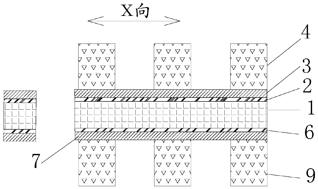
[0034] (3) Dry film lamination: form the upper dry film by lamination on the upper surface o...

Embodiment 2

[0043] The difference from Example 1 is: in step (4), the X-direction size of each upper and lower transparent area and the upper and lower dry film exposure part 4 is 4 microns, each upper and lower black area and the upper and lower The X-direction dimension of the unexposed part of the dry film is 10 microns.

Embodiment 3

[0045] The difference from Example 1 is: in step (1), the thickness of the upper and lower copper layers 3 is 0.5 micron; The dimensions in the X direction of each of the upper and lower black areas and the unexposed parts of the upper and lower dry films are all 8 microns in the X direction.


PUM

PropertyMeasurementUnit
thicknessaaaaaaaaaa
thicknessaaaaaaaaaa
thicknessaaaaaaaaaa

Abstract

The invention provides a method for manufacturing a COF double-sided flexible substrate fine circuit, comprising the following steps: (1) laser drilling; (2) in-hole metallization; (3) dry film pressing; (4) ultraviolet exposure of dry film; (5) dry film development; (6) electroplating copper; (7) stripping of dry film; 8) substrate copper layer etching; (9) metal Ni / Cr layer etching. The invention also provides a product obtained by the manufacturing method. A COF flexible double-sided substrate fine circuit with a copper thickness of about 10 micron and a linewidth / line spacing of up to 7 microns / 7 microns can be manufactured by adopting a semi-addition process and using a high-precision glass negative and a dry film with high adhesive force and high resolution.

Description

technical field [0001] The invention relates to a method for manufacturing a fine circuit of a COF double-sided flexible substrate and a product thereof. Background technique [0002] COF (Chip on film, chip on film technology), is to mount the chip on a flexible film substrate to realize the output of the chip I / O, and is widely used in the panels of mobile phones, TVs, ipads and other electronic products. At present, most of the companies that have mastered the production technology of COF flexible substrates and have the conditions for mass production are concentrated in South Korea, Japan, and Taiwan, China. Individual companies in mainland China have the production capacity of using etching methods to produce single-sided COF flexible substrates, but the minimum line width / line The distance does not reach the level of about 10 microns / 10 microns. With the rise of OLED in the panel industry, the demand for COF flexible substrates will increase. The difficulty of COF fl...

Claims


Application Information

Patent Timeline
Patent Type & Authority Patents(China)
IPC IPC(8): H05K3/00H05K3/06
CPCH05K3/0082H05K3/06H05K2203/052
Inventor 刘清万克宝张俊杰
Owner MFLEX YANCHENG CO LTD
Why Eureka
Try Eureka