Electrochromic device in freely customizable color and application
An electrochromic device and color technology, applied in instruments, nonlinear optics, optics, etc., can solve problems such as not easy to apply, no texture, not beautiful enough, etc., to improve product reliability, good surface texture, and shorten life Effect
- Summary
- Abstract
- Description
- Claims
- Application Information
AI Technical Summary
Problems solved by technology
Method used
Image
Examples
Embodiment 1
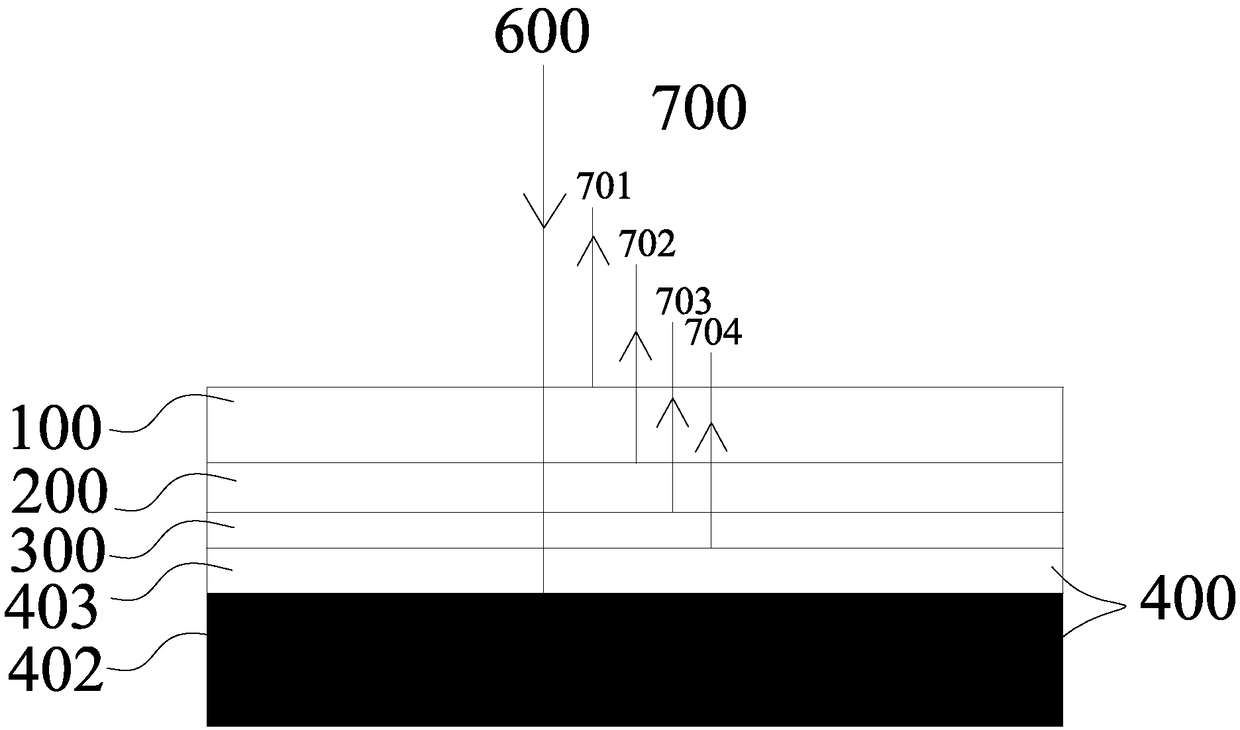
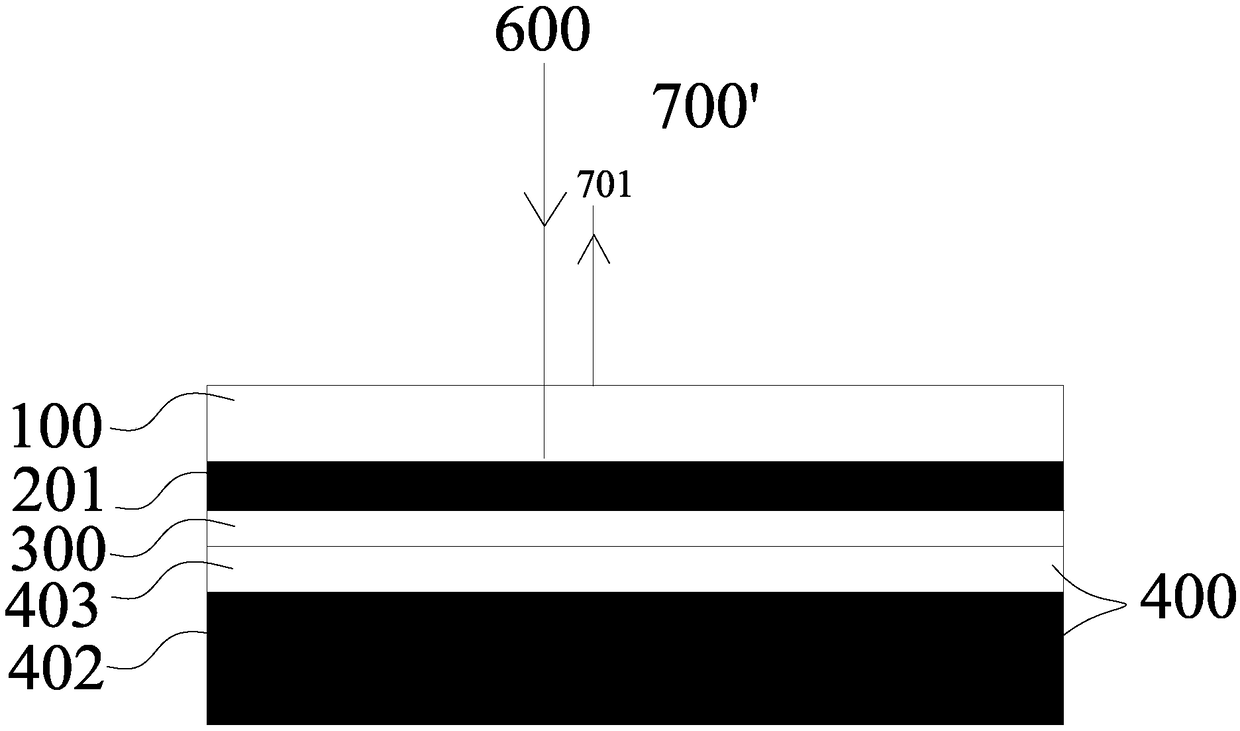
[0063] Such as figure 1 and 2 as shown, figure 1 It is a schematic diagram of the structure of the electrochromic device whose color can be customized arbitrarily in Example 1 before it changes color; figure 2 It is a schematic diagram of the structure of the electrochromic device whose color can be customized in Example 1 after it changes color; the electrochromic device in this embodiment is applied to the back cover of a mobile terminal (mobile phone), and various customized colors such as light blue become black, and the electrochromic The layered structure of the device is: transparent substrate layer 100 , EC stack 200 , optical film layer 300 , OCA optical adhesive layer 403 and black PET 402 . At present, six kinds of optical film layers 300 of film systems have been successfully tested, as shown in the table below.
[0064] Table 1 Light blue optical film system scheme
[0065] layers
Material
Thickness (nm)
1
TiO2
20.96
2
...
Embodiment 2
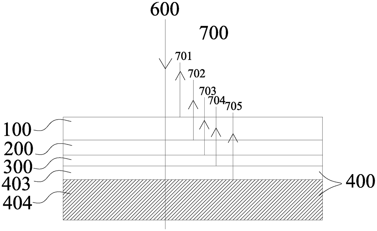
[0082] Such as image 3 and Figure 4 as shown, image 3 It is a schematic structural diagram before the color of the electrochromic device whose color can be customized in Example 2 before changing color, Figure 4 It is a structural schematic diagram of the electrochromic device whose color can be customized arbitrarily in Example 2; the electrochromic device of this embodiment is applied to the back cover of a mobile terminal (mobile phone), and the red color turns black, and the layered structure of the electrochromic device is as follows: : a transparent substrate layer 100 , an EC stack 200 , an optical film layer 300 , an OCA optical glue layer 403 and a color base layer 404 .
[0083] Table 7 Anti-reflection and anti-reflection optical film system scheme
[0084] layers
Material
Thickness (nm)
1
MgF2
92.66
2
ZrO2
131.72
3
MgF2
30.31
4
ZrO2
16.54
[0085] Before discoloration: the mobile termi...
Embodiment 3
[0088] Such as Figure 5 and Figure 6 as shown, Figure 5 It is a schematic structural diagram of the electrochromic device before the color of the embodiment 3 is arbitrarily customizable, Figure 6 It is a schematic diagram of the structure of the electrochromic device whose color can be customized in Example 3 after it changes color; the electrochromic device in this embodiment is applied to the back cover of the mobile terminal (PAD), and the blue color turns black, and the layered structure of the electrochromic device is sequentially They are: transparent substrate layer 100 , EC stack 200 , optical film layer 300 , and ink layer 405 , and the ink layer 405 of this embodiment is customized as blue ink.
[0089] Before discoloration: the mobile terminal does not power on the EC stack 200, so the incident light 600 can pass through the EC stack 200 and reach the ink layer 405. Before discoloration, the ink layer 405 is customized to be blue, and the ink layer 405 reflec...
PUM
 Abstract
Description
Claims
Application Information


