Infrared light emitting diode with strain compensation layer and manufacturing method thereof

A light-emitting diode and deformation compensation technology, which is applied to electrical components, circuits, semiconductor devices, etc., can solve problems such as deformation and efficiency drop

Inactive Publication Date: 2018-11-23
KODENSHI
View PDF0 Cites 0 Cited by
  • Summary
  • Abstract
  • Description
  • Claims
  • Application Information

AI Technical Summary

Problems solved by technology

[0003] However, this structure is deformed during the growth of InGaAs used as the quantum well of the active layer due to the inconsistency of the crystal lattice with the GaAs layer, resulting in a drop in efficiency.

Method used


Image

  • Infrared light emitting diode with strain compensation layer and manufacturing method thereof
  • Infrared light emitting diode with strain compensation layer and manufacturing method thereof
  • Infrared light emitting diode with strain compensation layer and manufacturing method thereof

Examples


Embodiment Construction

[0040] Hereinafter, the present invention will be described in detail through examples.

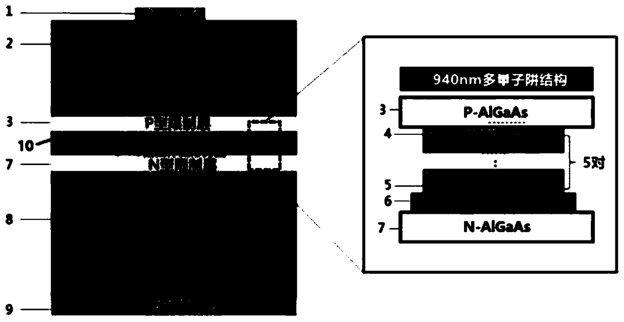
[0041] figure 1 shows applicable In x Ga 1-x 940nm infrared light emitting diode structure of P deformation compensation layer.

[0042] Such as figure 1 As shown, the structure of the 940nm infrared light-emitting diode is as follows: the n-type GaAs substrate 8 at the bottom, the Al substrate grown on the n-type GaAs substrate 0.3 Ga 0.7 An n-type confinement layer 7 made of As, and an In x Ga 1-x The deformation compensation layer 6 composed of P, on the deformation compensation layer 6 through the quantum barrier 5 composed of GaAs and the In 0.07Ga 0.93 The quantum wells 4 made of As are alternately grown five times to form the active layer 10, on which Al is grown 0.3 Ga 0.7 The p-type confinement layer 3 made of As, for the current diffusion effect of the infrared light emitting diode and the expansion effect of the emission cone area, a 5 μm-thick Al layer is grown on th...


PUM


Abstract

The invention relates to an infrared light emitting diode and a manufacturing method thereof, and more specifically relates to an infrared light emitting diode with improved light emitting efficiencyand a manufacturing method thereof. The infrared light emitting diode according to the present invention includes a GaAs substrate; a first type AlGaAs lower confinement layer grown on the GaAs substrate; an InGaP strain compensation layer grown on the first type AlGaAs lower confinement layer; an active layer including an InGaAs quantum well grown on the InGaP strain compensation layer; a secondtype AlGaAs upper confinement layer grown on the active layer; a window layer; and an electrode.

Description

technical field [0001] The present invention relates to an infrared light-emitting diode and a manufacturing method thereof, and more specifically, to an infrared light-emitting diode with improved luminous efficiency and a manufacturing method thereof. Background technique [0002] An infrared light-emitting diode with a center wavelength of 940±10nm (hereinafter referred to as a center wavelength of 940nm) is grown on a gallium arsenide (GaAs) substrate with a high lattice consistency rate and a high cost reduction (economic type). n-type AlGaAs (Al x Ga 1-x As) substance and p-type aluminum gallium arsenide (Al x Ga 1-x As) material (0.1<x<0.7), and has an active layer between the n-type material and the p-type material, and the active layer includes an undoped GaAs quantum barrier and an indium gallium arsenide (InGaAs) quantum well, so The indium (In) content of the InGaAs quantum wells is adjusted below 10% for growth on such layers (n-type, p-type or quantum...

Claims


Application Information

Patent Timeline
Patent Type & Authority Applications(China)
IPC IPC(8): H01L33/06H01L33/00
CPCH01L33/0062H01L33/06H01L33/0066H01L33/30H01L33/0025H01L33/12
Inventor 李亨株
Owner KODENSHI
Why Eureka
Try Eureka