
Optical element and method for manufacturing same, and optical modulator

A manufacturing method and technology for optical components, which are applied to optical components, optical waveguides and light guides, instruments, etc., can solve the problems of increased loss of high-order modes and increased loss of connecting fundamental modes.

Active Publication Date: 2018-11-23
FURUKAWA ELECTRIC CO LTD
View PDF6 Cites 2 Cited by
  • Summary
  • Abstract
  • Description
  • Claims
  • Application Information

AI Technical Summary

Problems solved by technology

As a result, the high-order modes are radiated toward the substrate side, resulting in an increase in the loss of the high-order modes.
[0004] On the other hand, in an optical waveguide with a high mesa structure, if the mesa width is too narrow to increase the high-order mode loss, even the fundamental mode loss will increase.

Method used


Image

  • Optical element and method for manufacturing same, and optical modulator
  • Optical element and method for manufacturing same, and optical modulator
  • Optical element and method for manufacturing same, and optical modulator

Examples


no. 1 approach

[0056] use Figure 1 to Figure 13 The optical element and its manufacturing method according to the first embodiment of the present invention will be described.

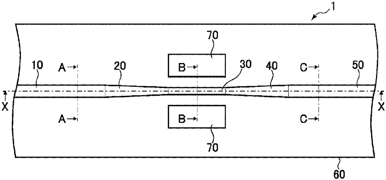
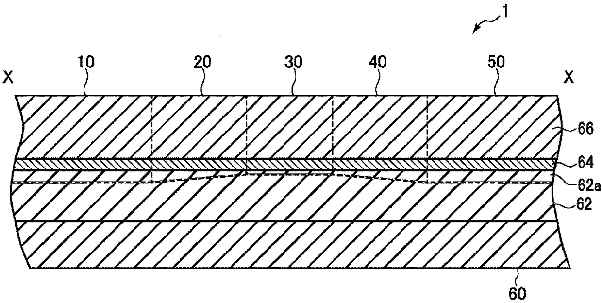
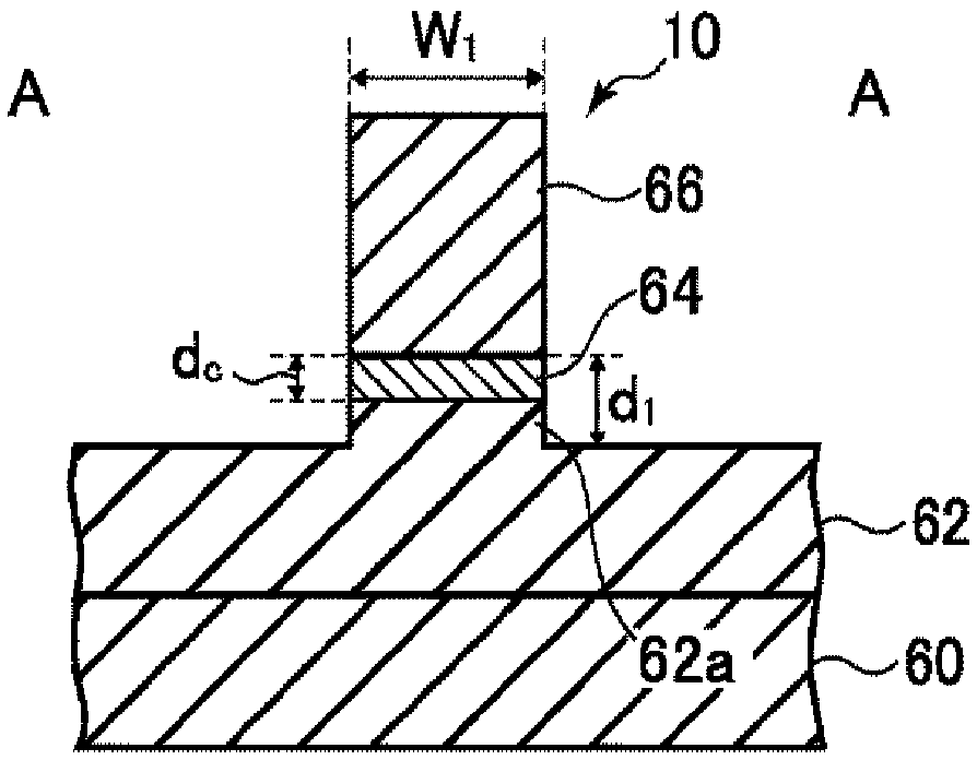
[0057] First, use Figures 1 to 4B The configuration of the optical element of this embodiment will be described. figure 1 It is a plan view showing the optical element of this embodiment. figure 2 is along figure 1 Cross-sectional view of the X-X line. Figure 3A is along figure 1 Sectional view of line A-A. Figure 3B is along figure 1 Sectional view of the B-B line. Figure 3C is along figure 1 Sectional view of line C-C. Figure 4A and Figure 4B It is a cross-sectional view showing another example of the cross-sectional shape that the high mesa structure of the optical waveguide can have.

[0058] The optical device of this embodiment functions as a high-order mode filter. The optical element of this embodiment can be integrated with an active element such as an optical modulator and other elements ...

no. 2 approach

[0133] use Figure 14 The optical element and its manufacturing method according to the second embodiment of the present invention will be described. Figure 14 is a cross-sectional view showing the third optical waveguide in the optical element of this embodiment. In addition, the same reference numerals are assigned to the same constituent elements as those of the optical element and its manufacturing method of the above-mentioned first embodiment, and description thereof will be omitted or simplified.

[0134] The basic structure of the optical element of this embodiment is substantially the same as that of the optical element 1 of the first embodiment. In the optical element of this embodiment, the third optical waveguide 30 has a high mesa structure formed in a mesa shape from the upper cladding layer 66 to the upper part of the core layer 64 . In this point, the optical element of this embodiment differs from the optical element 1 of the first embodiment in which the t...

no. 3 approach

[0142] use Figure 15A and Figure 15B An optical modulator according to a third embodiment of the present invention will be described. Figure 15A and Figure 15B It is a schematic diagram showing the optical modulator of this embodiment. In addition, the same reference numerals are assigned to the same components as those of the optical element and the manufacturing method thereof according to the above-mentioned first and second embodiments, and description thereof will be omitted or simplified.

[0143] The optical elements of the first and second embodiments described above can be integrated on a semiconductor substrate together with active elements such as an optical modulator and other elements to constitute an optical integrated element. In this embodiment, an example of such an optical integrated element will be described. Specifically, the optical modulator of this embodiment is a Mach-Zehnder type optical modulator, and has a plurality of optical elements 1 of t...


PUM


Abstract

Provided are an optical element which can be inexpensively and easily manufactured and which is capable of adequately reducing or removing a higher mode while keeping loss of a fundamental mode low, amethod for manufacturing the same, and an optical modulator. The present invention has a substrate and first through third optical waveguides formed on the substrate and each having a lower claddinglayer, a core layer, and an upper cladding layer, the core layer having a larger refractive index than the lower cladding layer and the upper cladding layer, the first optical waveguide being optically connected to the second optical waveguide, the second optical waveguide being optically connected to the third optical waveguide, the first through third optical waveguides having a mesa structure in which top parts of at least the upper cladding layer and the core layer protrude on the lower cladding layer, the core height of the third optical waveguide being less than the core height of the first optical waveguide, the core height being the height to the top surface of the core layer from bottom surfaces on both sides of the mesa structure or locations where the inclination of lateral surfaces of the mesa structure becomes discontinuous approaching the bottom surfaces, and the mesa width of the third optical waveguide being less than the mesa width of the first optical waveguide, the mesa width being the width of the middle of the core layer.

Description

technical field [0001] Optical element, manufacturing method of optical element, and optical modulator Background technique [0002] As an optical waveguide, a semiconductor optical waveguide formed on a semiconductor substrate and having a core layer and a cladding layer made of a semiconductor material is known. As a waveguide structure of a semiconductor optical waveguide in an optical functional element or the like, for example, a structure called a high mesa structure is used. An optical waveguide with a high mesa structure has a feature that the waveguide loss is small and the bending radius can be reduced. [0003] The optical waveguide with high mesa structure is difficult to suppress high-order transverse modes due to the very narrow cut-off mesa width. Therefore, optical waveguides with high mesa structures are usually designed to increase the loss of high-order modes. Specifically, the equivalent refractive index of the high-order mode is designed to be smaller...

Claims


Application Information

Patent Timeline
Patent Type & Authority Applications(China)
IPC IPC(8): G02B6/122G02B6/12G02B6/136G02F1/025
CPCG02F1/025G02F1/2257G02B6/14G02B6/1228G02F1/212G02B6/136G02B2006/12078G02B2006/12173
Inventor 斋藤裕介木本龙也
Owner FURUKAWA ELECTRIC CO LTD
Learn More