Fingerprint identification structure and display panel
A fingerprint recognition and display panel technology, applied in character and pattern recognition, acquisition/organization of fingerprints/palmprints, instruments, etc., can solve problems such as crosstalk of fingerprint recognition structures
- Summary
- Abstract
- Description
- Claims
- Application Information
AI Technical Summary
Problems solved by technology
Method used
Image
Examples
Embodiment 1
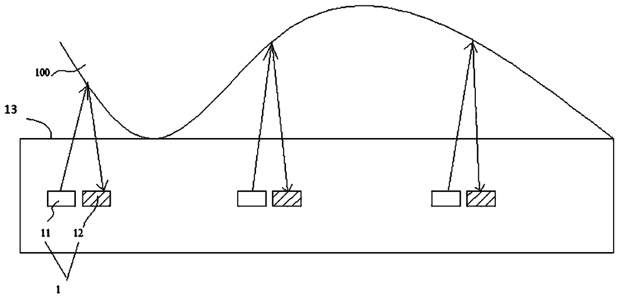
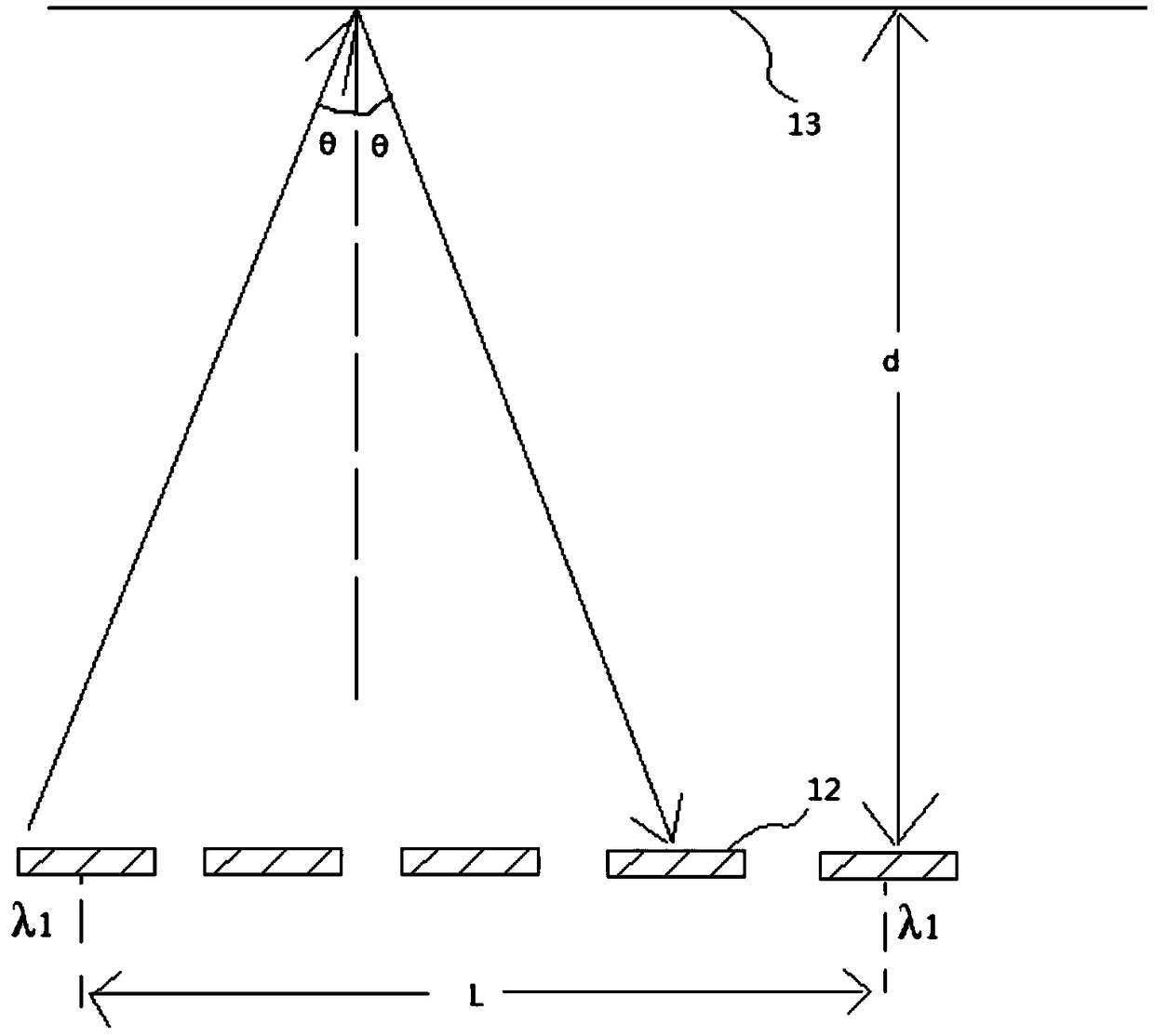
[0026] This embodiment provides a fingerprint identification structure, such as figure 1 and figure 2 As shown, it includes a plurality of identification units 1 arranged in an array; each identification unit 1 includes a transmitting module 11 and a sensing module 12, and the sensing module 12 is arranged to receive the emission emitted by the transmitting module 11 and reflected by the fingerprint 100. The position of the light that comes back; in each identification unit 1, the wavelength of the light that the sensing module 12 can sense is the same as the wavelength of the light emitted by the emission module 11; wherein, at least part of the emission module in the adjacent identification unit 1 11 The emitted light has different wavelengths.
[0027] The emitting module 11 and the sensing module 12 appear in pairs, and the sensing module 12 is used for sensing the light emitted by the corresponding emitting module 11 and reflected by the fingerprint 100 . The emitting ...
Embodiment 2
[0042] This embodiment provides a display panel including the fingerprint identification structure provided in Embodiment 1 of the present invention.
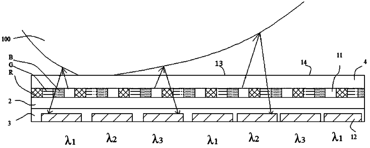
[0043] Specifically, in the display panel of this embodiment, the fingerprint identification structure provided by Embodiment 1 can be used as a relatively independent component, and it can be bonded together with the display substrate in the display panel by a method such as bonding, or it can be implemented The emission module 11 and / or the sensing module 12 in the fingerprint identification structure provided in Example 1 are integrated in the sub-pixel layer of the display panel.
[0044] Optionally, the display panel includes a first substrate 2, and an array of sub-pixels (including red sub-pixels R, Green sub-pixel G, blue sub-pixel B); the emission module 11 is arranged on the same layer as the sub-pixel and is arranged in the gap between adjacent sub-pixels, and / or, the sensing module 12 is arranged on the same layer a...
PUM
 Abstract
Description
Claims
Application Information


