Flexible panel and device with display panel

A flexible panel and flexible technology, applied in the direction of electrical components, electrical solid devices, circuits, etc., can solve the problems of reducing product life, increasing pressure drift in the channel area of ​​​​thin film transistors, and electrical degradation of thin film transistors, so as to improve the service life , weaken the electrical degradation, increase the effect of bending times

Active Publication Date: 2018-12-07
YUNGU GUAN TECH CO LTD
View PDF4 Cites 2 Cited by
  • Summary
  • Abstract
  • Description
  • Claims
  • Application Information

AI Technical Summary

Problems solved by technology

[0004] Therefore, the technical problem to be solved by the present invention is to overcome the fact that in the prior art, thin film transistors with a uniform channel design are still prone to stress defects in the stress concentration area of ​​the flexible display due to stress, which will cause electrical degradation of the thin film transistor and increase The problem of pressure drift in the channel region of thin film transistors, which reduces the service life of the product

Method used


Image

  • Flexible panel and device with display panel
  • Flexible panel and device with display panel
  • Flexible panel and device with display panel

Examples


Embodiment 1

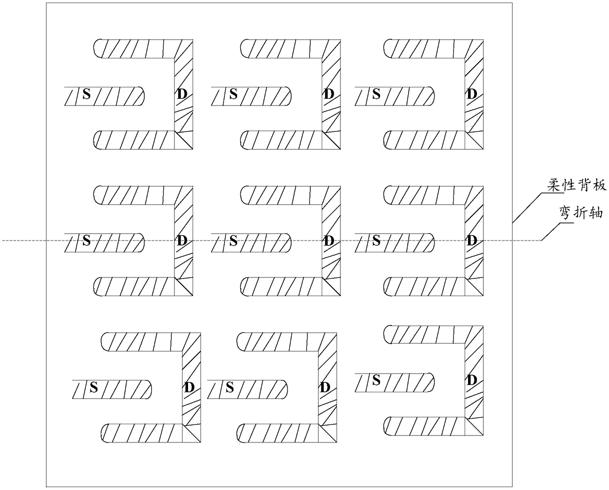
[0043] An embodiment of the present invention provides a flexible panel, such as figure 2 As shown, it includes a flexible backplane and several thin film transistors arranged in multiple arrays on the flexible backplane. Thin-Film-Transistor (TFT for short), thin-film transistor is one of the types of field-effect transistors, specifically, it can be an insulated gate field-effect transistor, and its production method is to deposit various thin films on the substrate, and its effect on display The performance of the device plays a very important role. Such as image 3 As shown, each thin film transistor includes a first electrode and a second electrode paired as a source and a drain, that is, the first electrode is a source S, and the second electrode is a drain D; or the first electrode is a drain D, The second electrode is the source S; a channel region is formed between the source S and the drain D, of course each thin film transistor also includes a gate G, the gate G ...

Embodiment 2

[0045] An embodiment of the present invention provides a flexible panel, such as figure 2 As shown, it includes a flexible backplane and several thin film transistors arranged in multiple arrays on the flexible backplane, each thin film transistor includes a first electrode and a second electrode, where the first electrode is the source S, The second electrode here is the drain D, a channel region is formed between the first electrode and the second electrode, and the flexible panel has a bending axis. At least one of the first electrode and the second electrode of the thin film transistor arranged along the bending axis overlaps the bending axis. Such as Figure 4 As shown, the bending axis only overlaps with the second electrode (drain) of the thin film transistor, and does not overlap with the first electrode (source). exist image 3 , the bending axes respectively overlap with the first electrode (source) and the second electrode (drain) of the thin film transistor. F...

Embodiment 3

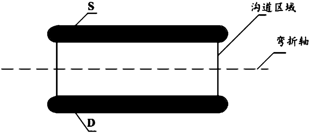
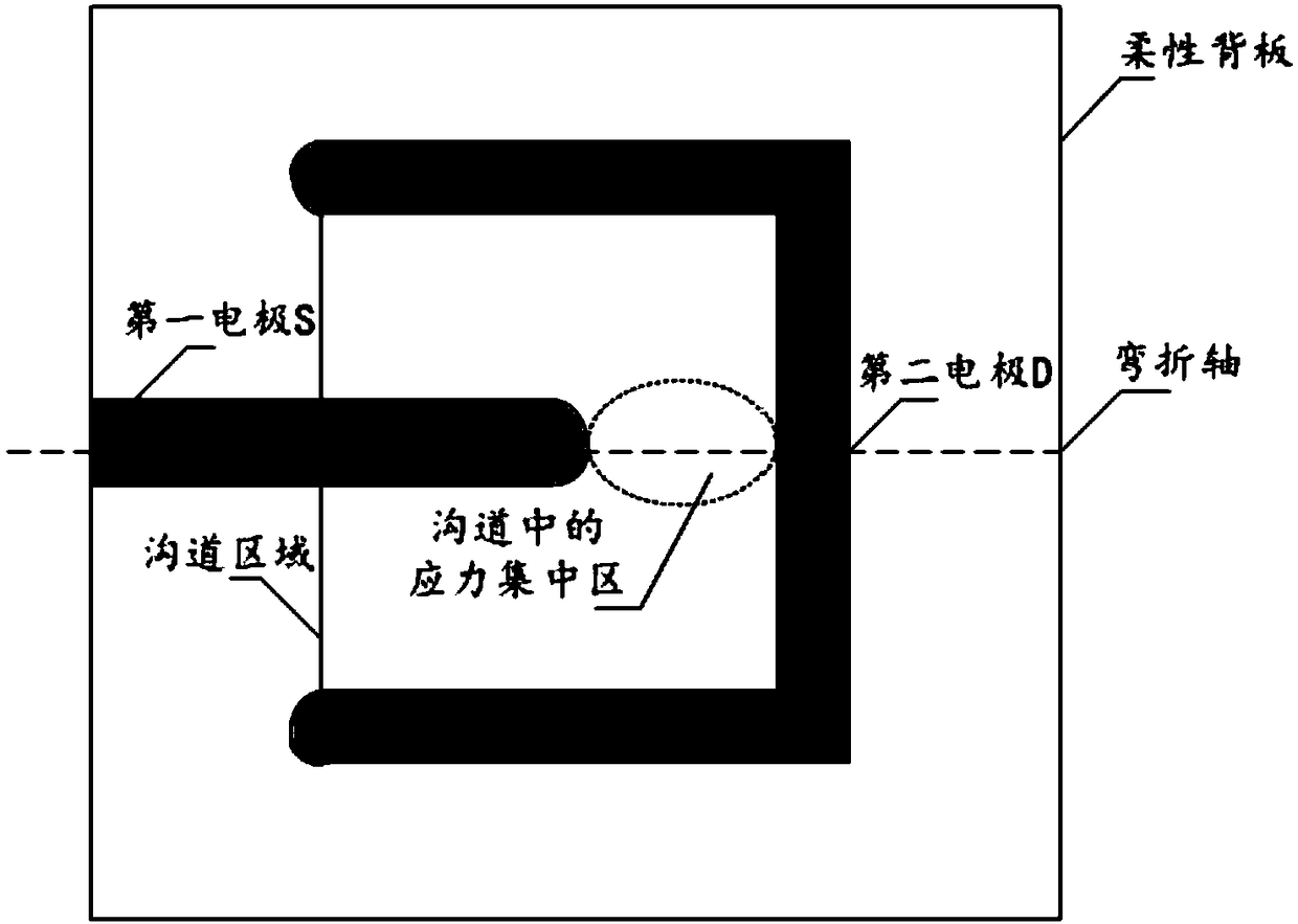
[0053] The present invention provides a flexible panel, including a flexible backplane and several thin film transistors arranged in multiple arrays on the flexible backplane, such as figure 2 As shown, each thin film transistor includes a source S and a drain D, and a channel region is formed between the source S and the drain D. Of course, each thin film transistor also includes a gate G, and the gate G is not in the figure 2 displayed in detail. exist figure 2 The bending axis of the flexible panel is located in the center of the channel region of the thin film transistor, and the axial area of ​​the bending axis of the flexible panel is a stress concentration area, which is more prone to stress defects when the flexible panel is bent. area, through figure 2 It can be seen that the stress concentration area in the non-uniform channel belongs to the partial area of ​​the non-uniform channel, and the area not in the axial direction of the bending axis of the flexible pa...


PUM


Abstract

The invention discloses a flexible panel and a device with a display panel. The flexible panel includes a flexible backplane and a plurality of thin film transistors arranged in multiple arrays on theflexible backplane. Each thin film transistor includes a first electrode and a second electrode which are paired as a source and a drain, and a channel region is formed between the first electrode and the second electrode. The flexible panel has a bending axis, and at least one of the first electrodes and the second electrodes of the multiple thin film transistors arranged along the bending axisoverlaps with the bending axis. The channel regions of the multiple thin film transistors arranged along the bending axis are non-uniform channels. Therefore, the electrical degradation of thin film transistors caused by stress can be weakened, the number of bending times of the flexible panel can be increased, and the service life of the flexible panel can be improved.

Description

technical field [0001] The invention relates to the field of display technology, in particular to a flexible panel and a device with a display panel. Background technique [0002] Transistors are key devices for making display devices, among which thin-film transistors (Thin-Film-Transistor, TFT for short) are electronic devices widely used in display devices. Since thin-film transistors are widely used in flexible and foldable products, the thin-film transistor Stability requirements are high, and the channel of the thin film transistor is prone to bending in the stress concentration area generated when the flexible panel is bent, resulting in stress defects, which affect the normal operation of the thin film transistor and light-emitting devices in the display device. [0003] At present, the traditional thin film transistor generally runs through the channel area of ​​the entire thin film transistor through the flexible display screen with its bending axis, so as to avoid...

Claims


Application Information

Patent Timeline
IPC IPC(8): H01L29/10H01L29/417H01L27/12
CPCH01L27/1214H01L27/1218H01L27/1222H01L29/1033H01L29/41733
Inventor 张立祥葛泳来宇浩翟智聪刘达金世遇冯奇
Owner YUNGU GUAN TECH CO LTD
Why Eureka
Try Eureka