Pixel structure and manufacturing method thereof

A technology of pixel structure and manufacturing method, which is applied in the direction of semiconductor devices, electrical components, circuits, etc., can solve the problems affecting the display contrast display effect of the display panel, lateral leakage current, etc., to optimize the display effect, prevent short-circuit phenomenon, and expand the deposition area Effect

Active Publication Date: 2021-07-20
GUANGDONG JUHUA PRINTING DISPLAY TECH CO LTD
View PDF4 Cites 0 Cited by
  • Summary
  • Abstract
  • Description
  • Claims
  • Application Information

AI Technical Summary

Problems solved by technology

However, when this structure is adopted, the functional layers of the sub-pixels in the same ink deposition area are integrated, which easily causes lateral leakage current, which in turn affects the display contrast and display effect of the entire display panel.

Method used


Image

  • Pixel structure and manufacturing method thereof
  • Pixel structure and manufacturing method thereof
  • Pixel structure and manufacturing method thereof

Examples


Embodiment

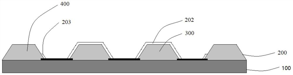
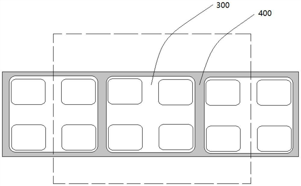
[0037] In this embodiment, a pixel structure, such as figure 1 and 2 shown, including:

[0038] Substrate 100;

[0039] The pixel defining layer 200 stacked on the substrate 100; the pixel defining layer 200 includes a first pixel bank300 and a second pixel bank400, and a plurality of sub-pixels surrounded by the first pixel bank300 and the second pixel bank400 corresponding to each sub-pixel pixel cavities; the pixel cavities on both sides of the first pixel bank300 are used to set sub-pixels with the same color, and the pixel cavities on both sides of the second pixel bank400 are used to set sub-pixels with different colors;

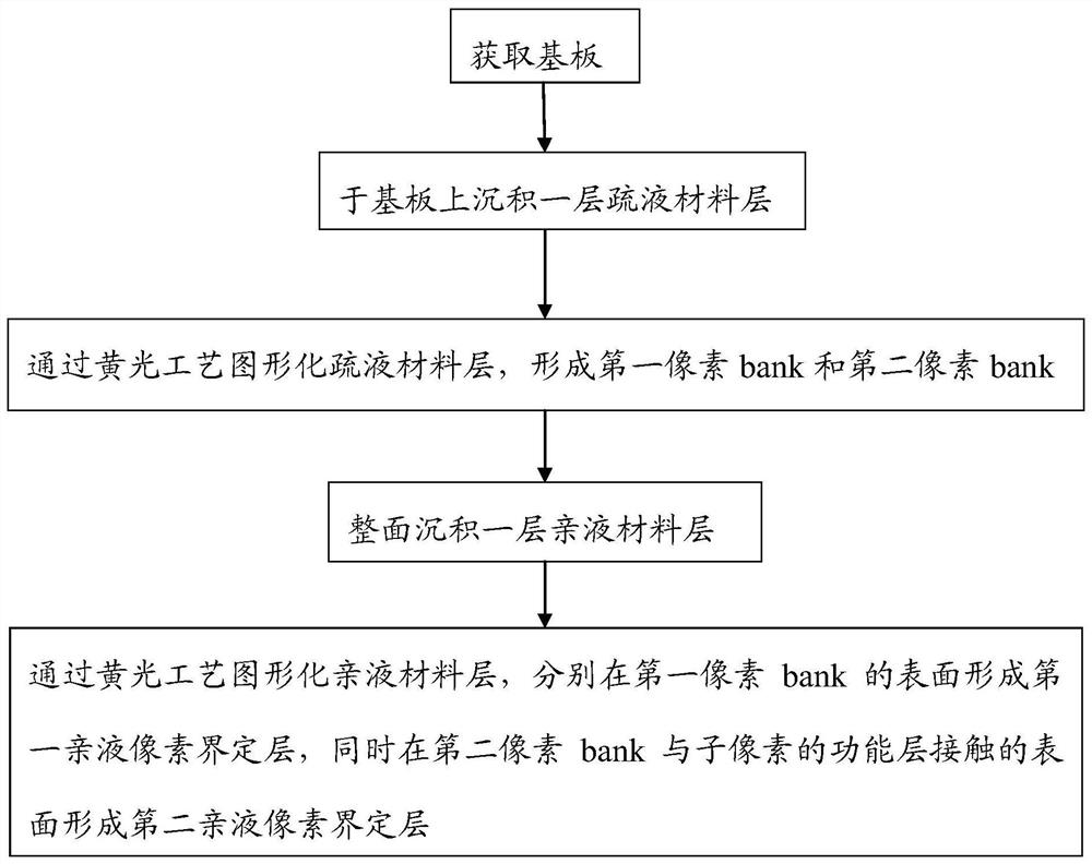
[0040] The surface of the first pixel bank 300 is provided with a first lyophilic pixel defining layer 202 . It can be understood that, in other embodiments, the first pixel bank 300 may also be entirely made of lyophilic materials, so that the surface thereof only needs to be lyophilic.

[0041] In the above pixel structure, the first lyophilic pi...


PUM

PropertyMeasurementUnit
thicknessaaaaaaaaaa
thicknessaaaaaaaaaa
thicknessaaaaaaaaaa

Abstract

The invention relates to a pixel structure and a manufacturing method thereof. The pixel structure includes: a substrate; a pixel definition layer laminated on the substrate; the pixel definition layer includes a first pixel bank and a second pixel bank, and the first pixel bank and the second pixel bank A plurality of pixel cavities corresponding to each sub-pixel are enclosed; the pixel cavities on both sides of the first pixel bank are used to set sub-pixels with the same color, and the pixel cavities on both sides of the second pixel bank are used to set Sub-pixels with different colors; the surface of the first pixel bank is provided with a first lyophilic pixel defining layer. The pixel structure can avoid the occurrence of leakage current between functional layers while realizing high-resolution printing, and optimize the display effect.

Description

technical field [0001] The invention relates to the field of display technology, in particular to a pixel structure and a manufacturing method thereof. Background technique [0002] Organic light-emitting diodes (OLEDs) and quantum dot light-emitting diodes (QLEDs) are the two main research directions of display devices at present. Organic electroluminescent diodes (OLEDs) have the advantages of self-illumination, fast response, wide viewing angle, high brightness, and thinness. Long and other advantages. The use of solution processing to manufacture OLED and QLED displays is an important direction for the development of future display technology due to its low cost, high productivity, and easy realization of large sizes. Among them, printing technology is considered to be the most effective way to realize OLED and QLED low-cost and large-area full-color display. [0003] In the printing process, through the optimization of the pixel arrangement structure, the sub-pixels ...

Claims


Application Information

Patent Timeline
Patent Type & Authority Patents(China)
IPC IPC(8): H01L27/32
CPCH10K59/122H10K59/1201
Inventor 陈亚文
Owner GUANGDONG JUHUA PRINTING DISPLAY TECH CO LTD
Why Eureka
Try Eureka