A light-emitting diode epitaxial wafer and its manufacturing method

A technology of light-emitting diodes and epitaxial wafers, applied in semiconductor devices, electrical components, nanotechnology, etc., can solve problems such as low luminous efficiency and limited luminous area, and achieve the effects of increasing luminous area, improving luminous brightness, and improving light extraction efficiency

Active Publication Date: 2020-09-08
HC SEMITEK ZHEJIANG CO LTD
View PDF4 Cites 0 Cited by
  • Summary
  • Abstract
  • Description
  • Claims
  • Application Information

AI Technical Summary

Problems solved by technology

[0006] The embodiment of the present invention provides a light-emitting diode epitaxial wafer and its manufacturing method, which can solve the problem of low luminous efficiency due to the limited light-emitting area in the prior art

Method used


Image

  • A light-emitting diode epitaxial wafer and its manufacturing method
  • A light-emitting diode epitaxial wafer and its manufacturing method
  • A light-emitting diode epitaxial wafer and its manufacturing method

Examples


Embodiment Construction

[0035] In order to make the object, technical solution and advantages of the present invention clearer, the implementation manner of the present invention will be further described in detail below in conjunction with the accompanying drawings.

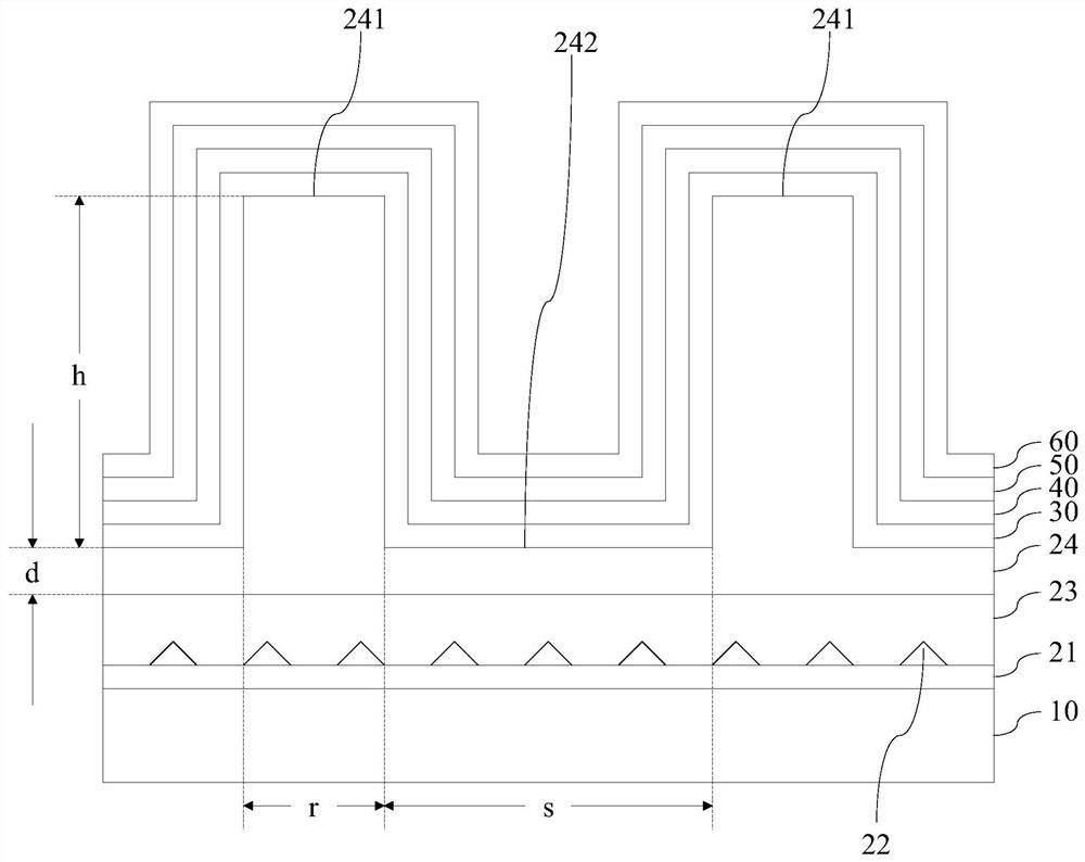
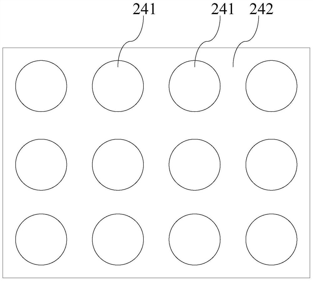
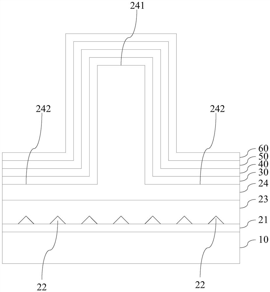
[0036] An embodiment of the present invention provides a light emitting diode epitaxial wafer, Figure 1a For a structural schematic diagram of a light-emitting diode epitaxial wafer provided in an embodiment of the present invention, see Figure 1a , the light-emitting diode epitaxial wafer includes a substrate 10, a low-temperature buffer layer 21, a three-dimensional nucleation layer 22, a two-dimensional recovery layer 23, an undoped gallium nitride layer 24, a reflective layer 30, an N-type semiconductor layer 40, an active layer 50 and P-type semiconductor layer 60. The low-temperature buffer layer 21, the three-dimensional nucleation layer 22 and the two-dimensional recovery layer 23 are sequentially stacked on the substrate 10, ...


PUM

PropertyMeasurementUnit
thicknessaaaaaaaaaa
heightaaaaaaaaaa
thicknessaaaaaaaaaa

Abstract

The invention discloses a light emitting diode epitaxial wafer and a manufacturing method thereof, belonging to the field of semiconductor technology. A light emit diode epitaxial wafer include a substrate, low temperature buffer layer, three-dimensional nucleation layer, two-dimensional recovery layer, An undoped gallium nitride lay, a reflective layer, an N-type semiconductor layer, an active layer and a P-type semiconductor layer, a low-temperature buffer layer, a three-dimensional nucleation layer and a two-dimensional recovery layer are sequentially laminated on the substrate, a first surface of an undoped gallium nitride layer is laid on the two-dimensional recovery layer, a second surface of the undoped gallium nitride layer comprises a convex portion and a concave portion, and thesecond surface is an opposite surface to the first surface; A light-reflecting layer is laid on the protrusion and the recess, and an N-type semiconductor layer, an active layer and a P-type semiconductor layer are laid on the light-reflecting layer in this order. The sum of the thicknesses of the P-type semiconductor layer, the active layer, the N-type semiconductor layer and the light-reflectinglayer is smaller than the height of the protrusion. The invention can increase the front light emission of the LED.

Description

technical field [0001] The invention relates to the technical field of semiconductors, in particular to a light-emitting diode epitaxial wafer and a manufacturing method thereof. Background technique [0002] A light-emitting diode (English: Light Emitting Diode, referred to as: LED) is a semiconductor electronic component that can emit light. LED has attracted wide attention due to its advantages of energy saving, environmental protection, high reliability, and long service life. For civil lighting, luminous efficiency and service life are the main criteria, so increasing the luminous efficiency of LEDs and improving the antistatic ability of LEDs is particularly critical for the wide application of LEDs. [0003] Epitaxial wafers are the primary products in the LED manufacturing process. The existing LED epitaxial wafer includes a substrate, a buffer layer, an N-type semiconductor layer, an active layer and a P-type semiconductor layer, and the buffer layer, the N-type s...

Claims


Application Information

Patent Timeline
Patent Type & Authority Patents(China)
IPC IPC(8): H01L33/06H01L33/10B82Y40/00H01L33/00H01L33/12H01L33/14H01L33/20H01L33/32
CPCB82Y40/00H01L33/007H01L33/06H01L33/10H01L33/12H01L33/145H01L33/20H01L33/32
Inventor 葛永晖郭炳磊王群吕蒙普胡加辉李鹏
Owner HC SEMITEK ZHEJIANG CO LTD
Why Eureka
Try Eureka